
HackPad

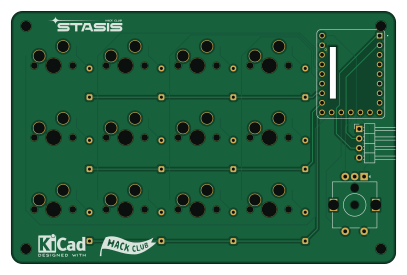
About the HackPad PCB
HackPad is an open source RP2040/RP2350 PCB design by ShlokVaidya, published on GitHub. It is a 2-layer board measuring 101.7 × 66.7 mm, with 26 components from 4 distinct parts.
Its main chip is the RP2040-ZERO, from the RP2040/RP2350 family. By type, the board carries 12 switches, 12 diodes, 1 IC and 1 connector.
It belongs with the keyboards designs in this gallery.
From the project
A 12-key macropad I built as my second hardware project for Stasis, designed to pair with my 60% keyboard for editing, shortcuts, media control, etc...
A 12-key macropad I built as my second hardware project for Stasis, designed to pair with my 60% keyboard for editing, shortcuts, media control, etc...
Hi there, this is my fully custom keypad from scratch, and I tried to keep it clean, practical, and actually buildable.
Note: The demo vid is working but u need to download to view it as it exceeds the 100mb Github limit.

Main components on the HackPad
HackPad bill of materials (BOM)
26 components, 4 distinct parts — part numbers from the project's BOM.
| Qty | Part | Footprint | Refs |
|---|---|---|---|
| 1 | RP2040-ZERO | MODULE_RP2040-ZERO | U1 |
| 1 | CONN_01X04_PIN Conn_01x04_Pin | PinHeader_1x04_P2.54mm_Horizontal | J1 |
| 12 | SW_PUSH_45DEG SW_Push_45deg | SW_MX_HS_KS-2P02B01-01_1u | SW1, SW2, SW3, SW4, SW5, SW6, SW7, SW8 +4 |
| 12 | 1N4148 | D_DO-35_SOD27_P7.62mm_Horizontal | D1, D2, D3, D4, D5, D6, D7, D8 +4 |
HackPad design files
The KiCad project lives in the ShlokVaidya/HackPad repository on GitHub; these links point at the commit this page was built from.
- LayoutPCB/HackPad.kicad_pcb
- SchematicPCB/HackPad.kicad_sch
- BOMproduction/bom.csv
HackPad: common questions
What microcontroller does the HackPad use?
The HackPad is built around the RP2040-ZERO, from the RP2040/RP2350 family.
How big is the HackPad PCB?
The HackPad measures 101.7 × 66.7 mm, has 2 copper layers and is 1.6 mm thick.
How many components are on the HackPad?
26 components, from 4 distinct parts, with part numbers taken from the project's own BOM. The full bill of materials is listed on this page.
Where can I download the HackPad design files?
From the ShlokVaidya/HackPad repository on GitHub, which has the KiCad layout, the schematic and the BOM; the links under Design files point to each one.
Can I use the HackPad design in my own project?
The repository has no license, so all rights stay with ShlokVaidya. Use it as a reference, and ask the author before reusing the design.
Can I test firmware for the HackPad without the hardware?
Yes. HardLabs builds a simulation of the board from its netlist and BOM, so you can run and debug RP2040/RP2350 firmware against it before you order a PCB.
Similar boards
 RP2040/RP2350
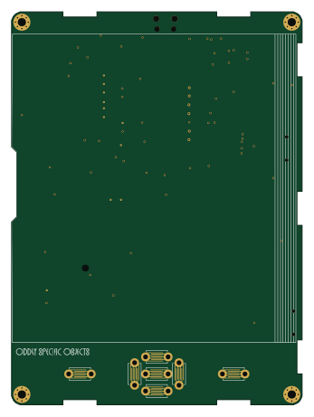
Open Book Abridged Edition
joeycastillo
85 × 115 mm29 parts2LCC-BY-SA-4.08.1k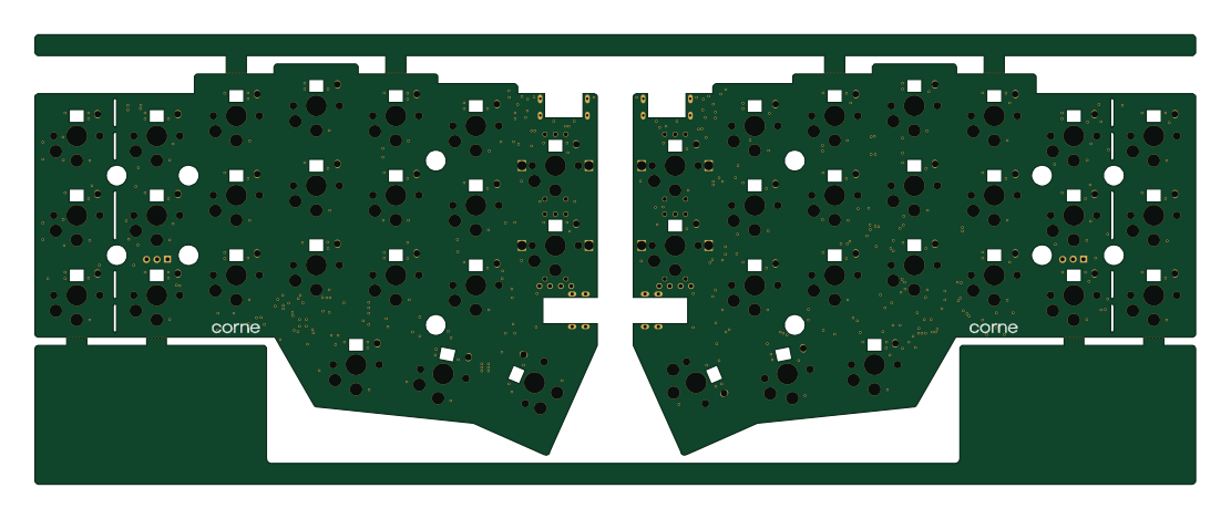 RP2040/RP2350
Corne
foostan
277.2 × 107.5 mm164 parts2LCC-BY-4.07.7k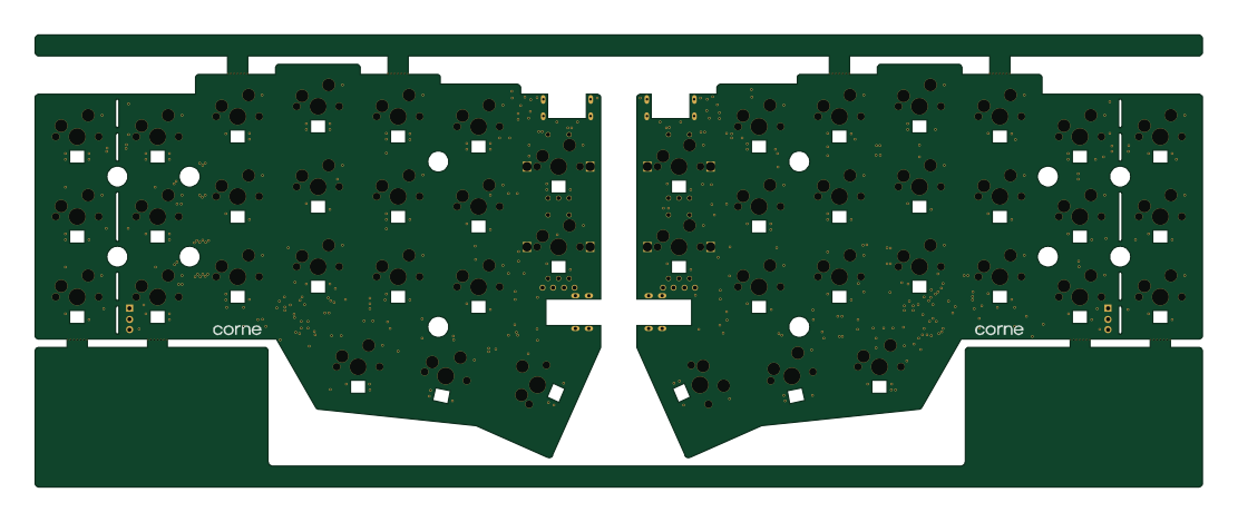 RP2040/RP2350
Corne
277.2 × 107.5 mm164 parts2LCC-BY-4.07.7k RP2040/RP2350
LogicAnalyzer
gusmanb
57 × 55.2 mm6 parts2LGPL-3.05.0k RP2040/RP2350
Jitx design
55.5 × 65 mm26 parts4LGPL-3.05.0k RP2040/RP2350
Pro V2
kata0510
290.1 × 130 mm270 parts2LMIT2.3k