
Vga timing 01

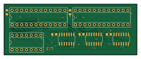
About the Vga timing 01 PCB
Vga timing 01 is an open source PCB design by sim82, published on GitHub under the MIT license. It is a 2-layer board measuring 70.6 × 26.9 mm, with 12 components from 5 distinct parts.
Other key parts include the 74LS393 and PAL20RS10. By type, the board carries 5 ICs, 5 capacitors, 1 crystal and 1 connector.
It belongs with the retro computing designs in this gallery.
Main components on the Vga timing 01
Vga timing 01 bill of materials (BOM)
12 components, 5 distinct parts.
| Qty | Part | Footprint | Refs |
|---|---|---|---|
| 3 | 74LS393 | SO-14_3.9x8.65mm_P1.27mm | U1, U2, U3 |
| 2 | PAL20RS10 | DIP-24_W7.62mm_Socket | U4, U5 |
| 1 | ACO-14MHz | DIP-14_W7.62mm_Socket | X1 |
| 1 | Conn_02x01 | PinSocket_2x01_P1.27mm_Vertical | J1 |
| 5 | 100nF | C_0805_2012Metric_Pad1.18x1.45mm_HandSolder | C1, C2, C3, C4, C5 |
Vga timing 01 design files
The KiCad project lives in the sim82/6502_sbc repository on GitHub; these links point at the commit this page was built from.
Vga timing 01: common questions
How big is the Vga timing 01 PCB?
The Vga timing 01 measures 70.6 × 26.9 mm, has 2 copper layers and is 1.6 mm thick.
How many components are on the Vga timing 01?
12 components, from 5 distinct parts. The full bill of materials is listed on this page.
Where can I download the Vga timing 01 design files?
From the sim82/6502_sbc repository on GitHub, which has the KiCad layout and the schematic; the links under Design files point to each one.
Can I use the Vga timing 01 design in my own project?
Yes, under the terms of its MIT license, which sim82 chose for the repository.
More boards in 6502_sbc
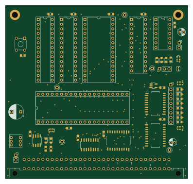
Cpu board 03
99.1 × 94.2 mm63 parts2LMIT1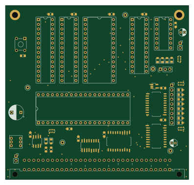
Cpu board 03 4l
99.1 × 94.2 mm62 parts4LMIT1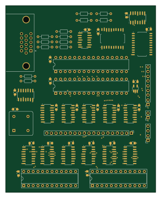
Vga mem output 01 4l
80.9 × 100.6 mm61 parts4LMIT1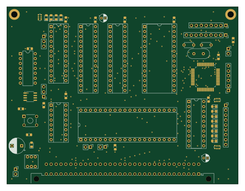
Cpu board 02
119.4 × 91.4 mm58 parts2LMIT1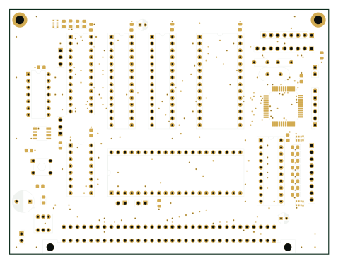
Pcb01 4l
119.4 × 91.4 mm58 parts4LMIT1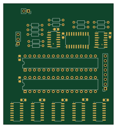
Vga mem output 01
59.4 × 65.5 mm34 parts2LMIT1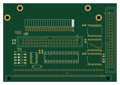
Hdctl 01
101.6 × 70.1 mm23 parts4LMIT1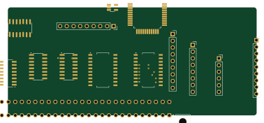
Com board 01
94.3 × 40.9 mm14 parts2LMIT1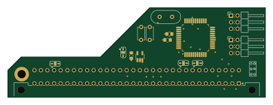
Min uart board 01
99.1 × 34.5 mm11 parts2LMIT1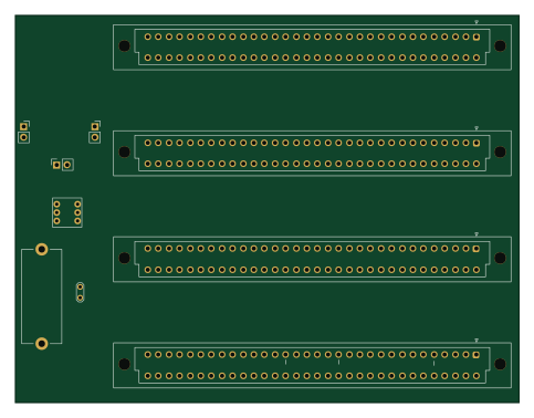
Backplane
120.7 × 92.7 mm10 parts2LMIT1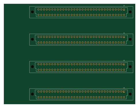
Io board 01
120.7 × 92.7 mm4 parts2LMIT1
Similar boards
Amiga External
hoglet67
21.9 × 76.7 mm6 parts2LGPL-3.01.0k
Atari pickup
26.4 × 53.9 mm7 parts2LGPL-3.01.0k
Deniseadapter
26.7 × 62.2 mm16 parts2LGPL-3.01.0k
Analog
53.9 × 23.2 mm33 parts2LGPL-3.01.0k
Rgb to hdmi
77 × 97 mm67 parts2LGPL-3.01.0k
Buffer
53.9 × 23.2 mm13 parts2LGPL-3.01.0k