
Kagura

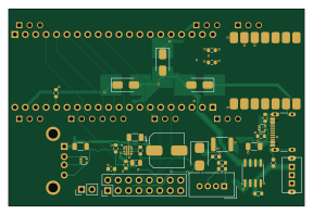
About the Kagura PCB
Kagura is an open source RP2040/RP2350 PCB design by siska-tech, published on GitHub under the Apache-2.0 license. It is a 4-layer board measuring 72 × 48 mm, with 44 components from 43 distinct parts.
Its main chip is the XIAO RP2040 SMD, from the RP2040/RP2350 family. Other key parts include the C3662799, TPD2E2U06DRLR and C1972959. By type, the board carries 13 connectors, 12 resistors, 7 capacitors, 4 ICs, 4 diodes and 1 transistor.
It belongs with the audio designs in this gallery.
From the project
Tang Nano 9K HDMI VDP and six-channel audio engine with SPI/QSPI host interfaces
Kinetic Audio & Graphics Unified Rendering Architecture。 Tang Nano 9K(GW1NR-9)1枚で動く、外部ホスト制御のHDMIビデオ・サウンドチップです。ホストは32 byteのレジスタ窓だけを操作し、FPGAが背景・spriteの描画、音源の合成、HDMI(映像+48kHz音声)出力を行います。
720pデモのRTLシミュレーション出力(論理320×180を1280×720へ4倍表示)。実機モニターの撮影ではありません。画像の生成元。
デモ動画(YouTube): KAGURA-9: Custom HDMI Video & 6-Channel Sound Chip
実機構成: Raspberry Pi Pico(SPI/QSPIホスト)とTang Nano 9K。配線はPico firmwareを参照。

Main components on the Kagura
Kagura bill of materials (BOM)
44 components, 43 distinct parts — part numbers from the project's BOM.
| Qty | Part | Footprint | Refs |
|---|---|---|---|
| 1 | XIAO RP2040 SMD | U1 | U1 |
| 1 | C3662799 TPS259470ARPWR / HOST LIMIT+RCB | U2 | U2 |
| 1 | TPD2E2U06DRLR | U4 | U4 |
| 1 | C1972959 TPD2E2U06DRLR / CC ESD | U5 | U5 |
| 1 | C16072 AO4407A / prototype | SOIC-8_3.9x4.9mm_P1.27mm | Q1 |
| 1 | 87520-0010BLF / Host | J2 | J2 |
| 1 | USB4105-GF-A / 5V3A POWER ONLY | J3 | J3 |
| 1 | GROVE I2C / 3V3 ONLY / 50mA SHARED | J4 | J4 |
| 1 | GPIO EXPANSION / 3V3 ONLY | J5 | J5 |
| 1 | 20 CONTACT SOCKET | J101 | J101 |
| 1 | 20 CONTACT SOCKET | J102 | J102 |
| 1 | SSW-103-01-G-S / Tang J5-1..3 | J201A | J2011 |
| 1 | SSW-106-01-G-S / Tang J5-6..11 | J201B | J2012 |
| 1 | SSW-103-01-G-S / Tang J5-14..16 | J201C | J2013 |
| 1 | SSW-103-01-G-S / Tang J5-20..22 | J201D | J2014 |
| 1 | SSW-103-01-G-S / Tang J6-1..3 | J202A | J2021 |
| 1 | SSW-103-01-G-S / Tang J6-18..20 | J202B | J2022 |
| 1 | SSW-103-01-G-S / Tang J6-22..24 | J202C | J2023 |
| 1 | C16490 MF-MSMF260/16X-2 / 2.6Ahold | F1 | F1 |
| 1 | HOST ENABLE / OPEN OFF | JP1 | JP1 |
Show 23 more
| Qty | Part | Footprint | Refs |
|---|---|---|---|
| 1 | SK-12D02-G040 / C2930976 | SW1 | SW1 |
| 1 | C8678 SS34 / MDD / Basic / Pico | D_SMA | D1 |
| 1 | C8678 SS34 / MDD / Basic / Tang | D_SMA | D2 |
| 1 | C8678 SS34 / MDD / Basic / XIAO | D_SMA | D3 |
| 1 | C19077561 SMBJ6.0CA-E3/52 / TRANSIENT ONLY | D4 | D4 |
| 1 | C28323 1u / 50V / X7R / 10% | C1 | C1 |
| 2 | C29823 4.7u / 50V / X7R / 10% | C_1206_3216Metric | C3, C5 |
| 1 | C401648 220u / 10V / 20% | C4 | C4 |
| 1 | C14663 100n / 16V / X7R | C6 | C6 |
| 1 | C14663 100n / 10V / GROVE | C7 | C7 |
| 1 | C53987 4.7n / 50V / X7R / 10% / dVdt | C8 | C8 |
| 1 | C23345 22 / 1% | R1 | R1 |
| 1 | C23345 22 / 1% | R2 | R2 |
| 1 | C25973 5.36k / 1% / ILM | R3 | R3 |
| 1 | C25803 100k / 1% / EN pulldown | R4 | R4 |
| 1 | C4410 1k / 1% / 0.25W | R5 | R5 |
| 1 | C23186 5.1k / 1% / CC1 Rd | R6 | R6 |
| 1 | C23186 5.1k / 1% / CC2 Rd | R7 | R7 |
| 1 | C23162 4.7k / 1% / SDA | R8 | R8 |
| 1 | C23162 4.7k / 1% / SCL | R9 | R9 |
| 1 | C25804 10k / 1% / IRQ bias | R10 | R10 |
| 1 | C25803 100k / 1% / EN feed | R11 | R11 |
| 1 | C25803 100k / 1% / gate pull-up | R_0603_1608Metric | R12 |
Kagura design files
The KiCad project lives in the siska-tech/kagura repository on GitHub; these links point at the commit this page was built from.
Kagura: common questions
What microcontroller does the Kagura use?
The Kagura is built around the XIAO RP2040 SMD, from the RP2040/RP2350 family.
How big is the Kagura PCB?
The Kagura measures 72 × 48 mm, has 4 copper layers and is 1.6 mm thick.
How many components are on the Kagura?
44 components, from 43 distinct parts, with part numbers taken from the project's own BOM. The full bill of materials is listed on this page.
Where can I download the Kagura design files?
From the siska-tech/kagura repository on GitHub, which has the KiCad layout, the schematic and the BOM; the links under Design files point to each one.
Can I use the Kagura design in my own project?
Yes, under the terms of its Apache-2.0 license, which siska-tech chose for the repository.
Can I test firmware for the Kagura without the hardware?
Yes. HardLabs builds a simulation of the board from its netlist and BOM, so you can run and debug RP2040/RP2350 firmware against it before you order a PCB.
Similar boards
 RP2040/RP2350
OSO-BOOK-C1
joeycastillo
85 × 115 mm29 parts2LCC-BY-SA-4.08.1k RP2040/RP2350
Corne cherry
foostan
277.2 × 107.5 mm164 parts2LCC-BY-4.07.7k RP2040/RP2350
Corne chocolate
277.2 × 107.5 mm164 parts2LCC-BY-4.07.7k RP2040/RP2350
Jitx design
gusmanb
55.5 × 65 mm26 parts4LGPL-3.05.0k RP2040/RP2350
LogicAnalyzer
57 × 55.2 mm6 parts2LGPL-3.05.0k RP2040/RP2350
Main
google
98 × 71 mm102 parts2LApache-2.02.9k