
IO-expander-MCP23017-breakout hardware design

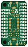
About the IO-expander-MCP23017-breakout hardware design
IO-expander-MCP23017-breakout hardware design is an open source PCB design by SolderedElectronics, published on GitHub under the TAPR-OHL-1.0 license. It is a 2-layer board measuring 22 × 38 mm, with 29 components from 15 distinct parts.
Other key parts include the MCP23017T-E_SS, NMOS-DUAL and SE5218. By type, the board carries 8 resistors, 7 jumpers, 7 relays, 3 ICs and 2 capacitors.
It belongs with the dev boards & breakouts designs in this gallery.
From the project
Hardware design, BOM, gerbers and 3D files for IO-expander-MCP23017-breakout designed by Soldered Electronics.
Are you short on IO pins? Looking to increase the number of them? That’s what the GPIO Expander MCP23017 is for! It uses I2C communication to do so. With just two wires, 16 new fully configurable digital IO pins are added to a microcontroller.
Due to the jumpers on the board, the I2C address of a device can be changed. Thus, eight breakout boards can be connected to a microcontroller. All of the pins on the expander board have pull-out resistors that can be turned on and off.

Main components on the IO-expander-MCP23017-breakout hardware design
IO-expander-MCP23017-breakout hardware design bill of materials (BOM)
29 components, 15 distinct parts — part numbers from the project's BOM.
| Qty | Part | Footprint | Refs |
|---|---|---|---|
| 1 | MCP23017T-E_SS | MCP23017 | U1 |
| 1 | NMOS-DUAL | SOT-363 | U2 |
| 1 | SE5218 | SOT-23-5 | U3 |
| 2 | HOLE_3.2mm | HOLE_3.2mm | H1, H2 |
| 2 | SMD_JUMPER_3_PAD_TRACE | SMD_JUMPER_3_PAD_TRACE | JP1, JP2 |
| 1 | SMD-JUMPER-CONNECTED_TRACE_SLODERMASK | SMD-JUMPER-CONNECTED_TRACE_SLODERMASK | JP3 |
| 1 | SMD_JUMPER | SMD_JUMPER | JP4 |
| 3 | SMD_JUMPER_3_PAD_CONNECTED_RIGHT | SMD_JUMPER_3_PAD_CONNECTED_RIGHT | JP5, JP6, JP7 |
| 2 | easyC-SMD | easyC-connector | K1, K3 |
| 1 | HEADER_MALE_4X1 | HEADER_MALE_4X1 | K2 |
| 2 | HEADER_MALE_8X1 | HEADER_MALE_8X1 | K4, K6 |
| 1 | HEADER_MALE_1X1 | HEADER_MALE_1X1 | K5 |
| 1 | HEADER_MALE_2X1 | HEADER_MALE_2X1 | K7 |
| 2 | 2.2uF | 0603C | C3, C4 |
| 8 | 10k | 0603R | R1, R2, R3, R4, R5, R6, R7, R8 |
IO-expander-MCP23017-breakout hardware design design files
The KiCad project lives in the SolderedElectronics/IO-expander-MCP23017-breakout-hardware-design repository on GitHub; these links point at the commit this page was built from.
IO-expander-MCP23017-breakout hardware design: common questions
How big is the IO-expander-MCP23017-breakout hardware design?
The IO-expander-MCP23017-breakout hardware design measures 22 × 38 mm, has 2 copper layers and is 1.6 mm thick.
How many components are on the IO-expander-MCP23017-breakout hardware design?
29 components, from 15 distinct parts, with part numbers taken from the project's own BOM. The full bill of materials is listed on this page.
Where can I download the IO-expander-MCP23017-breakout hardware design design files?
From the SolderedElectronics/IO-expander-MCP23017-breakout-hardware-design repository on GitHub, which has the KiCad layout, the schematic and the BOM; the links under Design files point to each one.
Can I use the IO-expander-MCP23017-breakout hardware design design in my own project?
Yes, under the terms of its TAPR-OHL-1.0 license, which SolderedElectronics chose for the repository.
Similar boards
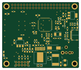
Radioberry juice
pa3gsb
65 × 56 mm87 parts2LNo license675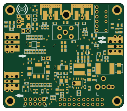
Radioberry preamp
65 × 56 mm137 parts2LNo license675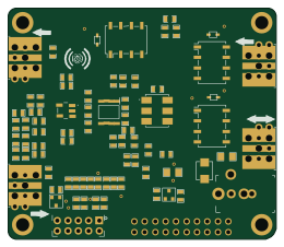
Hat
65 × 56 mm81 parts2LNo license675
Sram dev board
Wren6991
50 × 50 mm12 parts2LNo license508
ESP32
Chrismettal
66.4 × 48.1 mm20 parts2LCC-BY-SA-4.0446
ESP32
66.4 × 48.1 mm20 parts2LCC-BY-SA-4.0446