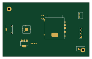
Spi flash adapter v1

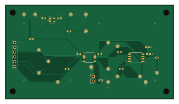
About the Spi flash adapter v1 PCB
Spi flash adapter v1 is an open source PCB design by Spectating101, published on GitHub under the MIT license. It is a 2-layer board measuring 90 × 50 mm, with 18 components from 10 distinct parts.
Other key parts include the TXU0304PWR, W25Q128JWSIQ and TLV75518PDBVR. By type, the board carries 7 resistors, 6 capacitors, 3 ICs, 1 connector and 1 jumper.
From the project
Auditable hardware bring-up: donor → KiCad carrier + DRC + bench gates → PROJECT_PACKAGE. Seeking 3 design partners.
This directory is the first complete Hardware Splicer reference design for the frozen 3.3 V-host to 1.8 V W25Q128JW case. It contains an editable KiCad 9 schematic, a routed two-layer PCB, an exact BOM, a machine-readable evidence/authority manifest, and scripts that regenerate, verify, and package the work without an external design contractor.
The current artifact is a bounded pre-fabrication result. It is internally consistent and reviewable, but it is not fabrication-authorized, power-on-authorized, or physically validated.
Main components on the Spi flash adapter v1
Spi flash adapter v1 bill of materials (BOM)
18 components, 10 distinct parts — part numbers from the project's BOM.
| Qty | Part | Footprint | Refs |
|---|---|---|---|
| 1 | TXU0304PWR Texas Instruments | TSSOP-14_4.4x5mm_P0.65mm | U1 |
| 1 | W25Q128JWSIQ Winbond Electronics | SOIC-8_5.3x5.3mm_P1.27mm | U2 |
| 1 | TLV75518PDBVR Texas Instruments | SOT-23-5 | U3 |
| 1 | TSW-106-07-T-S HOST_SPI_1x06 Samtec | PinHeader_1x06_P2.54mm_Vertical | J1 |
| 1 | TSW-102-07-T-S ENABLE_AFTER_RAIL_CHECK Samtec | PinHeader_1x02_P2.54mm_Vertical | JP1 |
| 2 | GRM188R71A105KA61D 1uF 10V X7R Murata | C_0603_1608Metric | C1, C6 |
| 1 | GRM188R60J475KE19D 4.7uF 6.3V X5R Murata | C_0603_1608Metric | C2 |
| 3 | GRM188R71C104KA01D 100nF 16V X7R Murata | C_0603_1608Metric | C3, C4, C5 |
| 2 | RC0603JR-070RL 0R Yageo | R_0603_1608Metric | R1, R4 |
| 5 | RC0603FR-0710KL 10k Yageo | R_0603_1608Metric | R2, R3, R5, R6, R7 |
Spi flash adapter v1 design files
The KiCad project lives in the Spectating101/hardware-splicer repository on GitHub; these links point at the commit this page was built from.
Spi flash adapter v1: common questions
How big is the Spi flash adapter v1 PCB?
The Spi flash adapter v1 measures 90 × 50 mm, has 2 copper layers and is 1.6 mm thick.
How many components are on the Spi flash adapter v1?
18 components, from 10 distinct parts, with part numbers taken from the project's own BOM. The full bill of materials is listed on this page.
Where can I download the Spi flash adapter v1 design files?
From the Spectating101/hardware-splicer repository on GitHub, which has the KiCad layout, the schematic and the BOM; the links under Design files point to each one.
Can I use the Spi flash adapter v1 design in my own project?
Yes, under the terms of its MIT license, which Spectating101 chose for the repository.