
Laya s hackpad

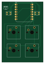
About the Laya s hackpad PCB
Laya s hackpad is an open source RP2040/RP2350 PCB design by Sreelaya-TS, published on GitHub. It is a 2-layer board measuring 43.2 × 63.3 mm, with 7 components from 3 distinct parts.
Its main chip is the XIAO-RP2040-DIP, from the RP2040/RP2350 family. By type, the board carries 4 switches, 2 diodes and 1 IC.
It belongs with the keyboards designs in this gallery.
From the project
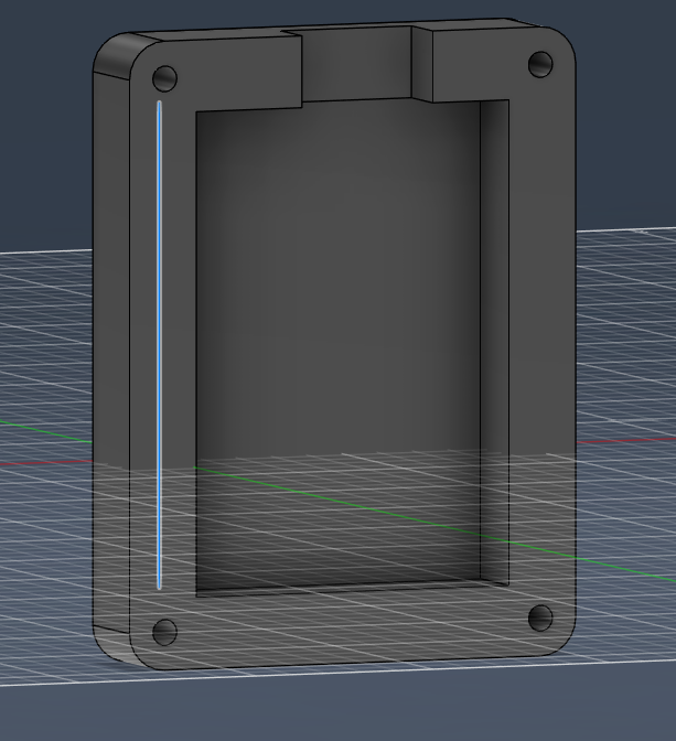
A custom-built 4-key macropad designed for coding shortcuts, powered by Seeed Studio XIAO RP2040, with a fully 3D-printed case and KMK firmware. honestly this was my first ever hardware project where i used the pcb editon and fusion 360 it was fun i had to google a lot of things
A custom-built 4-key macropad designed for coding shortcuts, powered by Seeed Studio XIAO RP2040, with a fully 3D-printed case and KMK firmware. honestly this was my first ever hardware project where i used the pcb editon and fusion 360 it was fun i had to google a lot of things and i tried to draw doreamon on back of my case it didnt extract well although i was succesfull in drawing a small robo on my pcb anyways i will continue working and learning abt it more this project taught me a lot than my traditional education could ever do
Main components on the Laya s hackpad
Laya s hackpad bill of materials (BOM)
7 components, 3 distinct parts.
| Qty | Part | Footprint | Refs |
|---|---|---|---|
| 1 | XIAO-RP2040-DIP | XIAO-RP2040-DIP | U1 |
| 4 | SW_Push | SW_Cherry_MX_1.00u_PCB | SW1, SW2, SW3, SW4 |
| 2 | SK6812MINI | LED_SK6812MINI_PLCC4_3.5x3.5mm_P1.75mm | D1, D2 |
Laya s hackpad design files
The KiCad project lives in the Sreelaya-TS/laya-s-hackpad repository on GitHub; these links point at the commit this page was built from.
- LayoutPCB/laya's macropad.kicad_pcb
- SchematicPCB/laya's macropad.kicad_sch
Laya s hackpad: common questions
What microcontroller does the Laya s hackpad use?
The Laya s hackpad is built around the XIAO-RP2040-DIP, from the RP2040/RP2350 family.
How big is the Laya s hackpad PCB?
The Laya s hackpad measures 43.2 × 63.3 mm, has 2 copper layers and is 1.6 mm thick.
How many components are on the Laya s hackpad?
7 components, from 3 distinct parts. The full bill of materials is listed on this page.
Where can I download the Laya s hackpad design files?
From the Sreelaya-TS/laya-s-hackpad repository on GitHub, which has the KiCad layout and the schematic; the links under Design files point to each one.
Can I use the Laya s hackpad design in my own project?
The repository has no license, so all rights stay with Sreelaya-TS. Use it as a reference, and ask the author before reusing the design.
Can I test firmware for the Laya s hackpad without the hardware?
Yes. HardLabs builds a simulation of the board from its netlist and BOM, so you can run and debug RP2040/RP2350 firmware against it before you order a PCB.
Similar boards
 RP2040/RP2350
OSO-BOOK-C1
joeycastillo
85 × 115 mm29 parts2LCC-BY-SA-4.08.1k RP2040/RP2350
Corne chocolate
foostan
277.2 × 107.5 mm164 parts2LCC-BY-4.07.7k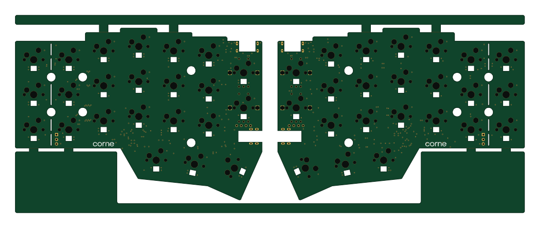 RP2040/RP2350
Corne cherry
277.2 × 107.5 mm164 parts2LCC-BY-4.07.7k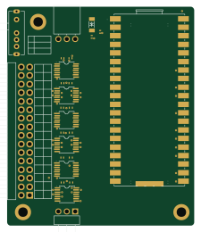 RP2040/RP2350
Jitx design
gusmanb
55.5 × 65 mm26 parts4LGPL-3.05.0k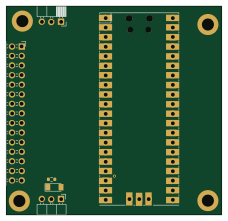 RP2040/RP2350
LogicAnalyzer
57 × 55.2 mm6 parts2LGPL-3.05.0k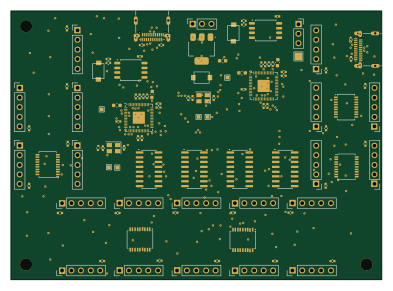 RP2040/RP2350
Main
google
98 × 71 mm102 parts2LApache-2.02.9k