
Smartphone-GNSS-Booster

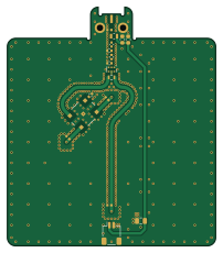
About the Smartphone-GNSS-Booster PCB
Smartphone-GNSS-Booster is an open source PCB design by taroz, published on GitHub under the MIT license. It is a 2-layer board measuring 50 × 57.5 mm, with 19 components from 15 distinct parts.
Other key parts include the X3C14P1-03S-1 and PD0922J5050S2HF. By type, the board carries 5 resistors, 4 diodes, 4 capacitors, 2 ICs, 2 connectors and 1 antenna.
It belongs with the rf & radio designs in this gallery.
From the project
Smartphone GNSS Booster
Smartphone-mounted GNSS signal re-radiator, designed in KiCad 10.
An external active GNSS antenna (Harxon HX-CU7603A or Beitian BT-230F, with its own LNA, powered through the coax by this board) is connected to the SMA input. The board splits the signal into L1 and L5 paths and feeds a dual-band patch antenna on the back side, which re-radiates the signal into the smartphone's internal GNSS antenna. The phone therefore receives a much cleaner signal than it would with its own antenna alone, which is what makes RTK with the android-rtcm-streamer app practical.
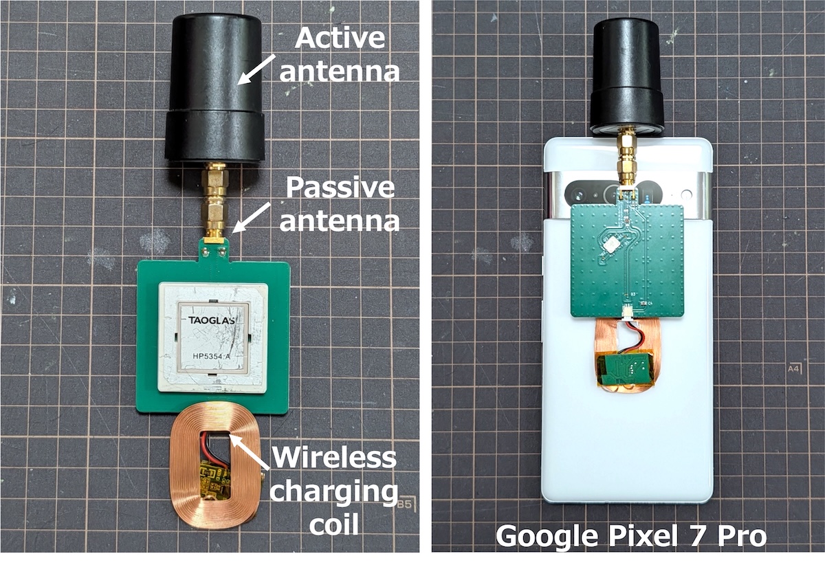
Main components on the Smartphone-GNSS-Booster
Smartphone-GNSS-Booster bill of materials (BOM)
19 components, 15 distinct parts — part numbers from the project's BOM.
| Qty | Part | Footprint | Refs |
|---|---|---|---|
| 1 | X3C14P1-03S-1 | RF_HybridCoupler_TTM_X3C14P1-03S | U1 |
| 1 | PD0922J5050S2HF | Xinger_0805_2012Metric-6_Pad0.33x0.41mm | U2 |
| 1 | C588468 Conn_Coaxial | SMA_Molex_732512440_Female_Embed | J1 |
| 1 | CONN_01X02_MOUNTINGPIN Conn_01x02_MountingPin | JST_SH_SM02B-SRSS-TB_1x02-1MP_P1.00mm_Horizontal | J2 |
| 1 | HP5354.A | Taoglas_HP5354.A_GNSS | AE1 |
| 4 | AXGD10402KR | D_Littelfuse_AXGD10402KR_0402_1005Metric_1.02x0.51mm | D1, D2, D3, D4 |
| 1 | LQW18ANR12G80D | L_Murata_LQW18ANxxxx80x_0603_1608Metric_1.65x0.99mm | L1 |
| 1 | GJM1555C1H470FB01D | C_Murata_xxx15_0402_1005Metric_1.0x0.5mm | C1 |
| 1 | 0.1U 0.1u | C_0603_1608Metric | C2 |
| 1 | 1u | C_0603_1608Metric | C3 |
| 1 | 10U 10u | C_0805_2012Metric | C4 |
| 1 | FCHP0402E50R0BGT1 | R_0402_1005Metric | R1 |
| 1 | FC0603E1000BTBST1 | R_Vishay_FC0603xxxxxxTxx_0603_1608Metric_1.626x0.813mm | R2 |
| 1 | 37 | R_0402_1005Metric | R3 |
| 2 | 150 | R_0402_1005Metric | R4, R5 |
Smartphone-GNSS-Booster design files
The KiCad project lives in the taroz/Smartphone-GNSS-Booster repository on GitHub; these links point at the commit this page was built from.
Smartphone-GNSS-Booster: common questions
How big is the Smartphone-GNSS-Booster PCB?
The Smartphone-GNSS-Booster measures 50 × 57.5 mm, has 2 copper layers and is 0.8 mm thick.
How many components are on the Smartphone-GNSS-Booster?
19 components, from 15 distinct parts, with part numbers taken from the project's own BOM. The full bill of materials is listed on this page.
Where can I download the Smartphone-GNSS-Booster design files?
From the taroz/Smartphone-GNSS-Booster repository on GitHub, which has the KiCad layout, the schematic and the BOM; the links under Design files point to each one.
Can I use the Smartphone-GNSS-Booster design in my own project?
Yes, under the terms of its MIT license, which taroz chose for the repository.
Similar boards
Radioberry preamp
pa3gsb
65 × 56 mm137 parts2LNo license675
Hat
65 × 56 mm81 parts2LNo license675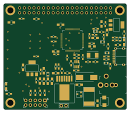
Radioberry juice
65 × 56 mm87 parts2LNo license675
Goodwatch20
travisgoodspeed
25.6 × 27.6 mm20 parts2LNo license568
Goodwatch31
25.6 × 27.6 mm23 parts2LNo license568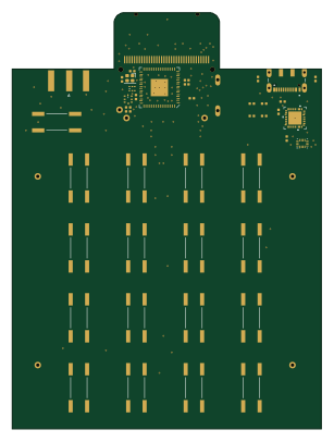
GoodPocketWatch
75.2 × 101.2 mm56 parts2LNo license568