
6 open source boards using the PD0922J5050S2HF
Real designs built with the PD0922J5050S2HF, from public GitHub projects: a quick way to see how others power, decouple and connect it. Each board comes with its KiCad files, full parts list and a render — and you can simulate its firmware on HardLabs.
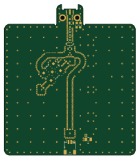
Smartphone-GNSS-Booster
taroz
50 × 57.5 mm19 parts2LMIT83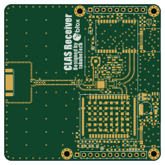
CLAS Combo Breakout
takuhoTech
60 × 60 mm80 parts4LMIT9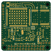
CelestNavi-HAT-for-ROCK-Pi-S
43.2 × 43.2 mm60 parts4LMIT5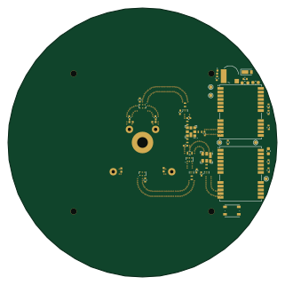
Antenna Module with integrated receiver
80 × 80 mm48 parts4LMIT0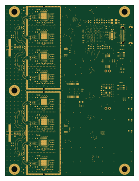
V4.1
tomojitakasu
70 × 92.8 mm221 parts4LBSD-3-Clause526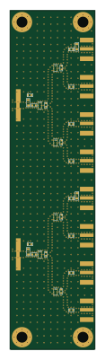
Div 4px2
25 × 100 mm42 parts4LBSD-3-Clause526
How designs wire the PD0922J5050S2HF
Read from the KiCad layouts of 5 open source designs, one per repository: what each pin of the PD0922J5050S2HF connects to, and the resistors, capacitors and other passives placed on it.
- The OUT1 pin has a series resistor on 5 of 5 designs, most often 100 Ω.
- The OUT2 pin has a series resistor on 5 of 5 designs, most often 100 Ω.
- The INPUT pin has a series capacitor on 2 of 5 designs, most often 100 pF.
| Pin | Connected to | Parts on the pin |
|---|---|---|
| GNDpin 1, 3, 5 | Connected to: GND 100% | — |
| INPUTpin 2 | Connected to: Signal 100% |
|
| OUT1pin 4 | Connected to: Signal 100% |
|
| OUT2pin 6 | Connected to: Signal 100% |
|
Connections count pins, parts count designs; values in brackets are how many parts had that value. Designs read include Div 4px2 by tomojitakasu, Smartphone-GNSS-Booster by taroz, CLAS Combo Breakout by takuhoTech and CelestNavi-HAT-for-ROCK-Pi-S by takuhoTech.
The PD0922J5050S2HF in open source designs
The gallery holds 6 open source boards using the PD0922J5050S2HF from 5 GitHub repositories; a typical one measures about 55 × 70 mm and carries around 54 components.
83% use four copper layers or more, and 100% carry an open source license.
The most starred is V4.1 by tomojitakasu.
Parts used alongside the PD0922J5050S2HF
What boards using the PD0922J5050S2HF are built for
PD0922J5050S2HF: common questions
Where can I find a PD0922J5050S2HF reference design?
Each of the 6 boards on this page is a real design using the PD0922J5050S2HF. Open one to see how it is wired up, with the full BOM, a render of the layout and links to its KiCad files.
What resistor goes on the PD0922J5050S2HF OUT1 pin?
The OUT1 pin has a series resistor on 5 of 5 designs, most often 100 Ω. Counted from the KiCad layouts of 5 open source designs using the PD0922J5050S2HF.
What resistor goes on the PD0922J5050S2HF OUT2 pin?
The OUT2 pin has a series resistor on 5 of 5 designs, most often 100 Ω. Counted from the KiCad layouts of 5 open source designs using the PD0922J5050S2HF.
How is the PD0922J5050S2HF INPUT pin connected?
The INPUT pin has a series capacitor on 2 of 5 designs, most often 100 pF. Counted from the KiCad layouts of 5 open source designs using the PD0922J5050S2HF.
How big is a typical board using the PD0922J5050S2HF?
The median is 55 × 70 mm, and 17% are two-layer designs.
What is the most popular open source board using the PD0922J5050S2HF?
By GitHub stars, V4.1 by tomojitakasu, with 526 stars.
Can I simulate one of these boards using the PD0922J5050S2HF before building it?
Yes. HardLabs turns a board's netlist and BOM into a working simulation, so you can boot and test firmware against it with no hardware on your desk.