
Soldered-IO-expander-MCP23017-breakout hardware design

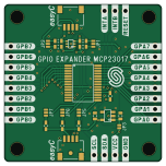
About the Soldered-IO-expander-MCP23017-breakout hardware design
Soldered-IO-expander-MCP23017-breakout hardware design is an open source PCB design by test-gh-syncer2, published on GitHub under the TAPR-OHL-1.0 license. It is a 2-layer board measuring 38 × 38 mm, with 30 components from 14 distinct parts.
Other key parts include the MCP23017T-E_SS, NMOS-DUAL and SE5218. By type, the board carries 8 resistors, 7 jumpers, 6 relays, 3 ICs and 2 capacitors.
It belongs with the dev boards & breakouts designs in this gallery.
From the project
Hardware design, BOM, gerbers, 3D files and pinout for IO-expander-MCP23017-breakout designed by Soldered.
Find XXXXXXXX on our [web store](https://solde.red/ .
All Soldered hardware is designed in KiCAD, and repositories are organised in the following way:
- CAD folder - contains KiCAD files (Schematics, Board, Panel Board), organised by version. Change log lists all changes between different versions. - OUTPUTS - contains useful files, such as Bill of Materials (BOM), PDF of schematics, 3D .step file of the board and gerber files, organised by version.
Main components on the Soldered-IO-expander-MCP23017-breakout hardware design
Soldered-IO-expander-MCP23017-breakout hardware design bill of materials (BOM)
30 components, 14 distinct parts — part numbers from the project's BOM.
| Qty | Part | Footprint | Refs |
|---|---|---|---|
| 1 | MCP23017T-E_SS | MCP23017 | U1 |
| 1 | NMOS-DUAL | SOT-363 | U2 |
| 1 | SE5218 | SOT-23-5 | U3 |
| 4 | HOLE_3.2MM HOLE_3.2mm | HOLE_3.2mm | H1, H2, H3, H4 |
| 2 | SMD_JUMPER_3_PAD_TRACE | SMD_JUMPER_3_PAD_TRACE | JP1, JP2 |
| 1 | SMD-JUMPER-CONNECTED_TRACE_SLODERMASK | SMD-JUMPER-CONNECTED_TRACE_SLODERMASK | JP3 |
| 1 | SMD_JUMPER | SMD_JUMPER | JP4 |
| 3 | SMD_JUMPER_3_PAD_CONNECTED_RIGHT | SMD_JUMPER_3_PAD_CONNECTED_RIGHT | JP5, JP6, JP7 |
| 2 | easyC-SMD | easyC-connector | K1, K3 |
| 1 | HEADER_MALE_4X1 | HEADER_MALE_4X1 | K2 |
| 2 | HEADER_MALE_8X1 | HEADER_MALE_8X1 | K4, K6 |
| 1 | HEADER_MALE_3X1 | HEADER_MALE_3X1 | K5 |
| 2 | 2.2UF 2.2uF | 0603C | C3, C4 |
| 8 | 10K 10k | 0603R | R1, R2, R3, R4, R5, R6, R7, R8 |
Soldered-IO-expander-MCP23017-breakout hardware design design files
The KiCad project lives in the test-gh-syncer2/Soldered-IO-expander-MCP23017-breakout-hardware-design repository on GitHub; these links point at the commit this page was built from.
Soldered-IO-expander-MCP23017-breakout hardware design: common questions
How big is the Soldered-IO-expander-MCP23017-breakout hardware design?
The Soldered-IO-expander-MCP23017-breakout hardware design measures 38 × 38 mm, has 2 copper layers and is 1.6 mm thick.
How many components are on the Soldered-IO-expander-MCP23017-breakout hardware design?
30 components, from 14 distinct parts, with part numbers taken from the project's own BOM. The full bill of materials is listed on this page.
Where can I download the Soldered-IO-expander-MCP23017-breakout hardware design design files?
From the test-gh-syncer2/Soldered-IO-expander-MCP23017-breakout-hardware-design repository on GitHub, which has the KiCad layout, the schematic and the BOM; the links under Design files point to each one.
Can I use the Soldered-IO-expander-MCP23017-breakout hardware design design in my own project?
Yes, under the terms of its TAPR-OHL-1.0 license, which test-gh-syncer2 chose for the repository.
Similar boards
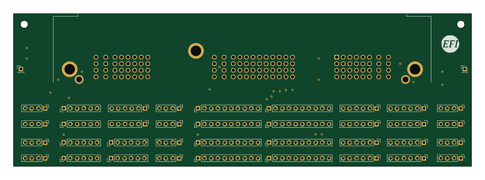
Breakout 112pin Connector
rusefi
174 × 58 mm39 parts2LGPL-3.01.2k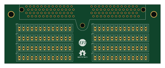
Eecv breakout
140.8 × 53.7 mm9 parts4LGPL-3.01.2k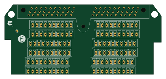
Breakout 60pin EEC-IV
139.7 × 62.2 mm15 parts2LGPL-3.01.2k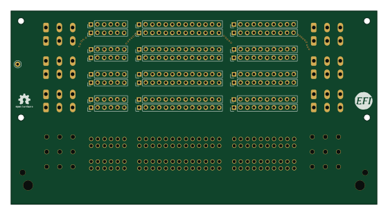
134pin 7-967288-1
139.7 × 73.7 mm38 parts2LGPL-3.01.2k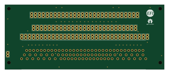
88 Pin Vag Breakout
142 × 58 mm91 parts2LGPL-3.01.2k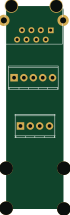
Rj45 breakout
rene-dev
15.2 × 53.8 mm3 parts2LGPL-3.0979