
Project wada

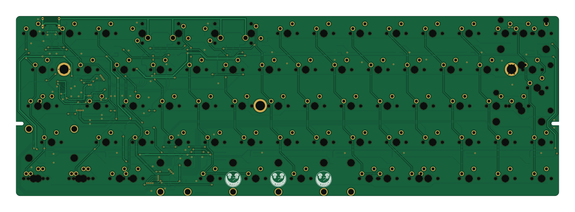
About the Project wada PCB
Project wada is an open source STM32 PCB design by ttran134, published on GitHub. It is a 2-layer board measuring 284.7 × 94.2 mm, with 244 components from 55 distinct parts.
Its main chip is the STM32F072C8T6, from the STM32 family. Other key parts include the XC6206PXXXMR, MIC2026-2BN, FE1.1, SRV05-4 and 74AHCT1G125. By type, the board carries 66 diodes, 47 capacitors, 16 LEDs, 13 resistors, 8 ICs and 7 switches.
It belongs with the keyboards and usb & debug tools designs in this gallery.
From the project
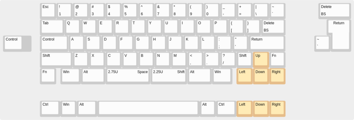
60% JIS like layout keyboard with USB hub
Although I love my HHKB Pro 2, sometimes I just want some arrow keys for gaming. This made me learn how to design a PCB and make it has a layout somewhat similar to the HHKB. I also realized that the Realforce RC1 kinda has the same layout as this keyboard too.
Main components on the Project wada
Project wada bill of materials (BOM)
244 components, 55 distinct parts — part numbers from the project's BOM.
| Qty | Part | Footprint | Refs |
|---|---|---|---|
| 1 | XC6206PXXXMR XC6206PxxxMR | SOT-23 | U1 |
| 1 | STM32F072C8T6 | LQFP-48_7x7mm_P0.5mm | U2 |
| 1 | MIC2026-2BN | SOIC-8_3.9x4.9mm_P1.27mm | U3 |
| 1 | FE1.1 | LQFP-48_7x7mm_P0.5mm | U4 |
| 3 | SRV05-4 | SOT-23-6-routable | U5, U6, U7 |
| 1 | 74AHCT1G125 | SOT-23-5 | U8 |
| 1 | 12MHZ 12MHz | Crystal_SMD_3225-4pin_3.2x2.5mm | Y1 |
| 1 | USB_C_RECEPTACLE_USB2.0_16P USB_C_Receptacle_USB2.0_16P | USB_C_Receptacle_HRO_TYPE-C-31-M-12 | J1 |
| 2 | C42646 USB_A | JING 903-231A2031S10100 | J2, J3 |
| 2 | SW_SPST | SW_SPST_TL3342 | BOOT_SW1, RESET_SW1 |
| 1 | 500MA 500mA | Fuse_1206_3216Metric | F1 |
| 1 | PCB Outline | GH60_outline_without_bottom_mounting | H1 |
| 50 | MX_SW_solder | SW_MX_1u | MX1, MX2, MX3, MX4, MX5, MX6, MX7, MX8 +42 |
| 1 | PIPE | SW_MX_1u | MX14 |
| 1 | TILDE | SW_MX_1u | MX15 |
| 1 | MX_SW_solder | SW_MX_1.5u | MX16 |
| 1 | BSHIT_HHKB | SW_MX_1.5u | MX29 |
| 1 | LCTRL | SW_MX_1.75u | MX30 |
| 1 | ANSI_ENTER | SW_MX_1u | MX42 |
| 1 | FN | SW_MX_1u | MX57 |
Show 35 more
| Qty | Part | Footprint | Refs |
|---|---|---|---|
| 1 | WIN | SW_MX_1.25u | MX58 |
| 2 | ALT | SW_MX_1.5u | MX59, MX62 |
| 1 | 275_SPACE | SW_MX_1u | MX60 |
| 1 | 225_SPACE | SW_MX_1u | MX61 |
| 1 | CTRL | SW_MX_1.25u | MX63 |
| 1 | LEFT | SW_MX_1u | MX64 |
| 1 | DOWN | SW_MX_1u | MX65 |
| 1 | RIGHT | SW_MX_1u | MX66 |
| 1 | BSHIT_TOP | SW_MX_1u | MX67 |
| 1 | alt_LCTRL | SW_MX_1.75u_STP_1.25 | MX68 |
| 1 | ISO_ENTER | SW_MX_1u | MX69 |
| 1 | ISO_PIPE | SW_MX_1u | MX70 |
| 1 | alt_CTRL | SW_MX_1.25u | MX71 |
| 1 | alt_WIN | SW_MX_1u | MX72 |
| 2 | alt_ALT | SW_MX_1.25u | MX73, MX75 |
| 1 | alt_625_SPACE | SW_MX_1u | MX74 |
| 1 | alt_CTRL | SW_MX_1u | MX76 |
| 1 | ANSI_2.25U | STAB_MX_2.25u | S1 |
| 1 | 2U | STAB_MX_P_2u | S2 |
| 1 | 2.75U | STAB_MX_P_2.75u | S3 |
| 1 | 2.25U | STAB_MX_P_2.25u | S4 |
| 1 | ISO_2U | STAB_MX_ISO-ROT | S5 |
| 1 | 6.25U | STAB_MX_P_6.25u | S6 |
| 1 | 2U | STAB_MX_2u | S7 |
| 16 | SK6812MINI | LED_SK6812MINI_HAND_SOLDER_3.5x3.5mm_P1.75mm | LED1, LED2, LED3, LED4, LED5, LED6, LED7, LED8 +8 |
| 66 | C81598 D_Small | D_SOD-123 | D1, D2, D3, D4, D5, D6, D7, D8 +58 |
| 3 | C85832 220V @ 100MHz, 2A | L_0603_1608Metric | L1, L2, L3 |
| 4 | 1UF 1uF | C_0603_1608Metric | C1, C9, C10, C11 |
| 4 | 10UF 10uF | C_0603_1608Metric | C2, C3, C24, C27 |
| 35 | 100NF 100nF | C_0603_1608Metric | C4, C5, C6, C7, C8, C12, C13, C14 +27 |
| 2 | 30PF 30pF | C_0603_1608Metric | C21, C22 |
| 2 | 100UF 100uF | CP_Elec_6.3x5.9 | C25, C28 |
| 2 | 5.1KR 5.1kR | R_0402_1005Metric | R1, R2 |
| 10 | 10KR 10kR | R_0603_1608Metric | R3, R4, R6, R7, R8, R9, R10, R11 +2 |
| 1 | 2.7KR 2.7kR | R_0603_1608Metric | R13 |
Project wada design files
The KiCad project lives in the ttran134/project_wada repository on GitHub; these links point at the commit this page was built from.
Project wada: common questions
What microcontroller does the Project wada use?
The Project wada is built around the STM32F072C8T6, from the STM32 family.
How big is the Project wada PCB?
The Project wada measures 284.7 × 94.2 mm, has 2 copper layers and is 1.6 mm thick.
How many components are on the Project wada?
244 components, from 55 distinct parts, with part numbers taken from the project's own BOM. The full bill of materials is listed on this page.
Where can I download the Project wada design files?
From the ttran134/project_wada repository on GitHub, which has the KiCad layout, the schematic and the BOM; the links under Design files point to each one.
Can I use the Project wada design in my own project?
The repository has no license, so all rights stay with ttran134. Use it as a reference, and ask the author before reusing the design.
Can I test firmware for the Project wada without the hardware?
Yes. HardLabs builds a simulation of the board from its netlist and BOM, so you can run and debug STM32 firmware against it before you order a PCB.
Similar boards
 STM32
LumenPnP Motherboard
opulo-inc
149 × 95 mm296 parts4LCC-BY-SA-4.03.7k STM32
Type g
google
169 × 30 mm24 parts2LApache-2.02.9k STM32
Base
52.3 × 52.3 mm36 parts2LApache-2.02.9k STM32
Main panel
234 × 84 mm26 parts4LApache-2.02.9k STM32
Type a
150 × 30 mm14 parts2LApache-2.02.9k STM32
Type c
188 × 30 mm17 parts2LApache-2.02.9k