
HackPad

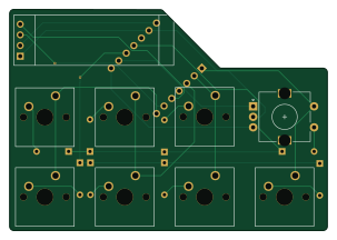
About the HackPad PCB
HackPad is an open source Microchip SAM PCB design by UKASITECH, published on GitHub. It is a 2-layer board measuring 75.5 × 52.6 mm, with 18 components from 5 distinct parts.
Its main chip is the Seeed Studio XIAO SAMD21, from the Microchip SAM family. By type, the board carries 8 switches, 8 diodes, 1 IC and 1 LED.
It belongs with the keyboards designs in this gallery.
From the project
A custom USB macropad with programmable keys for coding, productivity, and media controls. I will design the enclosure, PCB, and firmware from scratch.
built by Umang Kumar Singh for HackClub 2026
Hackpad is my first crack at a hardware project — a simple macropad with seven keys and a rotary encoder. Seven keys for whatever macros you want (calculator hotkey, anyone?), and the encoder handles volume or media scrubbing.
The body is two 3D-printed shells held together with M3 screws and heat-set inserts, with a translucent acrylic plate sandwiched in between. The plate can be swapped out pretty easily if you ever want to change the look.
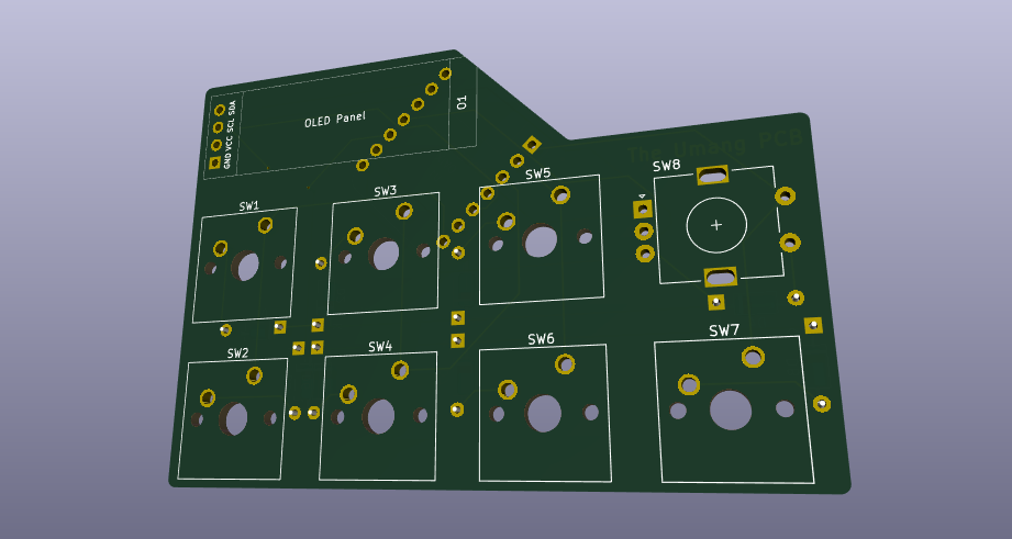
Main components on the HackPad
HackPad bill of materials (BOM)
18 components, 5 distinct parts — part numbers from the project's BOM.
| Qty | Part | Footprint | Refs |
|---|---|---|---|
| 1 | Seeed Studio XIAO SAMD21 | XIAO-Generic-Thruhole-14P-2.54-21X17.8MM | U1 |
| 7 | SW_PUSH_45DEG SW_Push_45deg | SW_Cherry_MX_1.00u_PCB | SW1, SW2, SW3, SW4, SW5, SW6, SW7 |
| 1 | RotaryEncoder_Switch | RotaryEncoder_Alps_EC11E-Switch_Vertical_H20mm | SW8 |
| 1 | OLEd | SSD1306-0.91-OLED-4pin-128x32 | O1 |
| 8 | D | D_DO-35_SOD27_P7.62mm_Horizontal | D1, D2, D3, D4, D5, D6, D7, D8 |
HackPad design files
The KiCad project lives in the UKASITECH/HackPad repository on GitHub; these links point at the commit this page was built from.
- Layoutpcb/hackpad.kicad_pcb
- Schematicpcb/hackpad.kicad_sch
- BOMproduction/bom.csv
HackPad: common questions
What microcontroller does the HackPad use?
The HackPad is built around the Seeed Studio XIAO SAMD21, from the Microchip SAM family.
How big is the HackPad PCB?
The HackPad measures 75.5 × 52.6 mm, has 2 copper layers and is 1.6 mm thick.
How many components are on the HackPad?
18 components, from 5 distinct parts, with part numbers taken from the project's own BOM. The full bill of materials is listed on this page.
Where can I download the HackPad design files?
From the UKASITECH/HackPad repository on GitHub, which has the KiCad layout, the schematic and the BOM; the links under Design files point to each one.
Can I use the HackPad design in my own project?
The repository has no license, so all rights stay with UKASITECH. Use it as a reference, and ask the author before reusing the design.
Can I test firmware for the HackPad without the hardware?
Yes. HardLabs builds a simulation of the board from its netlist and BOM, so you can run and debug Microchip SAM firmware against it before you order a PCB.
Similar boards
 Microchip SAM
Microcontroller Expansion Card
FrameworkComputer
26 × 30 mm24 parts2LCC-BY-4.01.1k Microchip SAM
Taco Raven
VoronDesign
120 × 113 mm349 parts4LGPL-3.01.1k Microchip SAM
Fpgaboy
Wren6991
50 × 50 mm89 parts4LNo license511 Microchip SAM
OpenDropV4
GaudiLabs
124 × 115.4 mm118 parts2LGPL-3.0487 Microchip SAM
ModulAdapter universal
100 × 69.5 mm45 parts2LGPL-3.0487 Microchip SAM
Kira
kiibohd
366.9 × 114.3 mm400 partsCERN-OHL-1.2416