
IP5328P-powerbank design

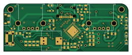
About the IP5328P-powerbank design PCB
IP5328P-powerbank design is an open source PCB design by YC-Lam, published on GitHub under the GPL-3.0 license. It is a 2-layer board measuring 65 × 25 mm, with 47 components from 23 distinct parts.
Other key parts include the IP5328. By type, the board carries 19 capacitors, 10 resistors, 5 diodes, 4 transistors, 4 connectors and 1 IC.
It belongs with the power & battery designs in this gallery.
From the project
a USB power delivery powerbank pcb based on IP5328P chip, feel free to use it
- support QC2.0/QC3.0 output - Support FCP input/output - Support AFC input/output - Support SFCP input/output - Support MTK PE1.1&2.0 output - Support USB C DRP input/output - Support BC1.2, Apple, Samsung - Support PD2.0 bi-directional input/output protocol - Support PD3.0 input/output and PPS output protocol - Support 5V@3.1A, 9V@2.0A, 12V@1.5A voltage output
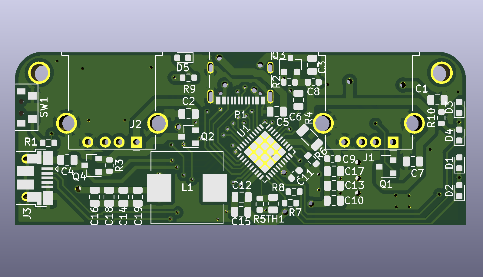
Main components on the IP5328P-powerbank design
IP5328P-powerbank design bill of materials (BOM)
47 components, 23 distinct parts.
| Qty | Part | Footprint | Refs |
|---|---|---|---|
| 1 | IP5328 | QFN-40-1EP_6x6mm_P0.5mm_EP4.6x4.6mm | U1 |
| 2 | RU207C | SOT-23 | Q1, Q2 |
| 2 | RU20P7C | SOT-23 | Q3, Q4 |
| 2 | USB_A | USB_A_Stewart_SS-52100-001_Horizontal | J1, J2 |
| 1 | USB_B_Micro | USB_Micro-B_Amphenol_10103594-0001LF_Horizontal | J3 |
| 1 | USB_C_Plug_USB2.0 | USB_C_Receptacle_Palconn_UTC16-G | P1 |
| 1 | Battery_Cell | bat | BT1 |
| 1 | SW_Push | FPC_2 | SW1 |
| 1 | 100k@25c | R_0805_2012Metric | TH1 |
| 5 | LED | LED_0603_1608Metric | D1, D2, D3, D4, D5 |
| 1 | 2.2uh | L_Wuerth_HCI-1040 | L1 |
| 5 | 10uf 25v | C_0805_2012Metric | C1, C2, C3, C4, C17 |
| 2 | 2.2uf 16v | C_0805_2012Metric | C5, C6 |
| 5 | 22uf 25v | C_0805_2012Metric | C7, C10, C12, C13, C15 |
| 3 | 100nf 25v | C_0603_1608Metric | C8, C9, C11 |
| 4 | 22uf 16v | C_0805_2012Metric | C14, C16, C18, C19 |
| 1 | 1k | R_0603_1608Metric | R1 |
| 2 | 10k | R_0603_1608Metric | R2, R3 |
| 1 | 0.01R | R_1206_3216Metric | R4 |
| 1 | 82k 1% | R_0603_1608Metric | R5 |
Show 3 more
| Qty | Part | Footprint | Refs |
|---|---|---|---|
| 1 | 114k | R_0603_1608Metric | R6 |
| 3 | 100R | R_0603_1608Metric | R7, R8, R9 |
| 1 | NC | R_0603_1608Metric | R10 |
IP5328P-powerbank design design files
The KiCad project lives in the YC-Lam/IP5328P-powerbank_design repository on GitHub; these links point at the commit this page was built from.
- Layoutusbpd_powerbank.kicad_pcb
- Schematicusbpd_powerbank.kicad_sch
IP5328P-powerbank design: common questions
How big is the IP5328P-powerbank design PCB?
The IP5328P-powerbank design measures 65 × 25 mm, has 2 copper layers and is 1.6 mm thick.
How many components are on the IP5328P-powerbank design?
47 components, from 23 distinct parts. The full bill of materials is listed on this page.
Where can I download the IP5328P-powerbank design design files?
From the YC-Lam/IP5328P-powerbank_design repository on GitHub, which has the KiCad layout and the schematic; the links under Design files point to each one.
Can I use the IP5328P-powerbank design design in my own project?
Yes, under the terms of its GPL-3.0 license, which YC-Lam chose for the repository.
Similar boards

Stack chan
stack-chan
50 × 50 mm33 parts2LApache-2.01.7k
Display Carrier
AxxAxx
35.6 × 58.2 mm5 parts2LGPL-3.01.7k
ControllerCurrentShuntAddOn
stuartpittaway
26 × 16.9 mm9 parts2LCC-BY-NC-4.01.1k
Module 16S PassiveBalanceAddOn
61 × 74 mm86 parts2LCC-BY-NC-4.01.1k
TemperaturePCB PANEL
116 × 75.5 mm178 parts2LCC-BY-NC-4.01.1k
ProgrammingAdapter
10.5 × 83 mm3 parts2LCC-BY-NC-4.01.1k