
Pereda choc

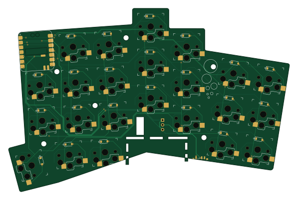
About the Pereda choc PCB
Pereda choc is an open source Nordic nRF PCB design by YikeStone, published on GitHub under the CERN-OHL-S-2.0 license. It is a 2-layer board measuring 148.9 × 97.5 mm, with 51 components from 7 distinct parts.
Its main chip is the 101991463, from the Nordic nRF family. By type, the board carries 23 diodes and 1 IC.
It belongs with the keyboards, iot & wireless and power & battery designs in this gallery.
From the project
Pereda is a custom wireless mechanical keyboard designed for Kailh Choc V1 switches.
Pereda is a custom wireless mechanical keyboard designed for Kailh Choc V1 switches.
It has 46 keys, aggressive column stagger, and column splay. The key positions are designed around my finger length and natural finger-joint movement rather than a conventional keyboard layout.
Kailh Choc V1 switches Seeed Studio XIAO nRF52840 Wireless 46 keys Aggressive column stagger and column splay Reversible PCB 301230 LiPo battery, 120 mAh Magnetic USB-C connector for charging * Custom ergonomic key layout
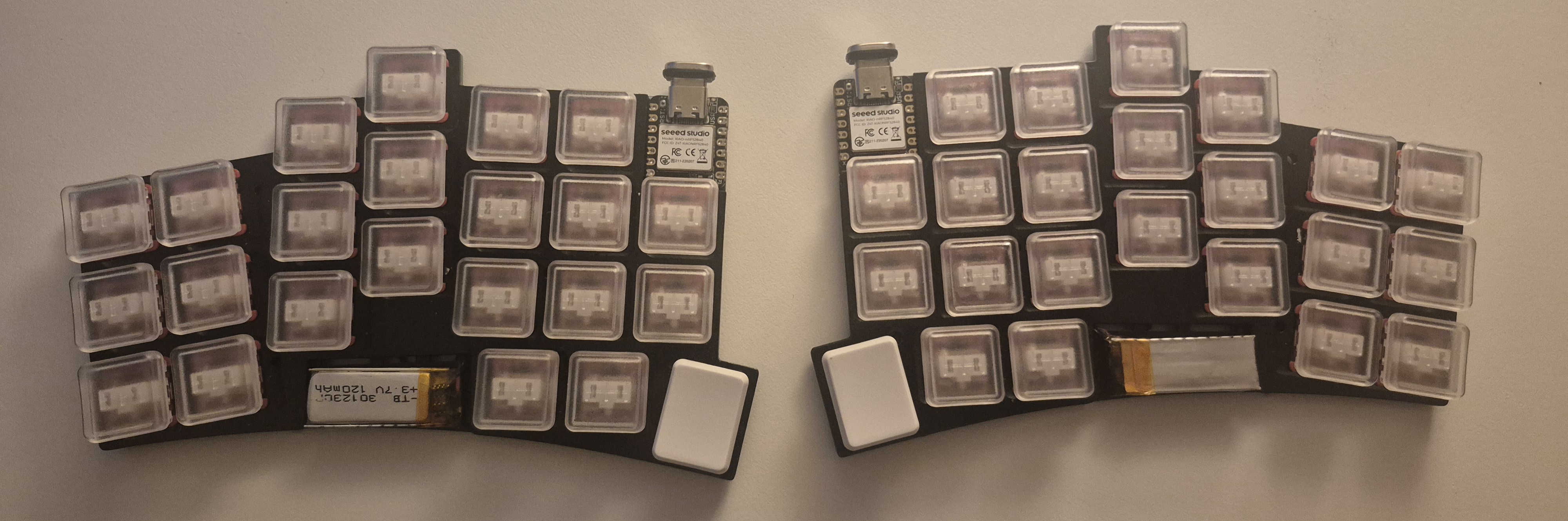
Main components on the Pereda choc
Pereda choc bill of materials (BOM)
51 components, 7 distinct parts — part numbers from the project's BOM.
| Qty | Part | Footprint | Refs |
|---|---|---|---|
| 1 | 101991463 XIAO-nRF52840-SMD Seeed Technology Co., Ltd | XIAO-nRF52840-SMD-kbd | U1 |
| 2 | PCM12SMTBR SPDT | SW_SPDT_PCM12 | SMDSW2, rSMDSW1 |
| 1 | M50-3930342 Conn_01x03 | PinHeader_1x03_P2.54mm_Horizontal | rJ2 |
| 1 | 5118 SW_Push | Kailh_socket_PG1350_reversible_1.25u | rSW1 |
| 22 | 5118 SW_Push | Kailh_socket_PG1350_reversible_1u | rSW2, rSW3, rSW4, rSW5, rSW6, rSW7, rSW8, rSW9 +14 |
| 1 | 101991463 XIAO-nRF52840-SMD Seeed Technology Co., Ltd | XIAO-nRF52840-SMD-kbd | rU6 |
| 23 | 1N4148W 1N4148WT Diotec Semiconductor | D_SOD-123-rev | D2, D3, D4, D5, D6, D7, D8, D9 +15 |
Pereda choc design files
The KiCad project lives in the YikeStone/pereda-kbd repository on GitHub; these links point at the commit this page was built from.
Pereda choc: common questions
What microcontroller does the Pereda choc use?
The Pereda choc is built around the 101991463, from the Nordic nRF family.
How big is the Pereda choc PCB?
The Pereda choc measures 148.9 × 97.5 mm, has 2 copper layers and is 1.6 mm thick.
How many components are on the Pereda choc?
51 components, from 7 distinct parts, with part numbers taken from the project's own BOM. The full bill of materials is listed on this page.
Where can I download the Pereda choc design files?
From the YikeStone/pereda-kbd repository on GitHub, which has the KiCad layout, the schematic and the BOM; the links under Design files point to each one.
Can I use the Pereda choc design in my own project?
Yes, under the terms of its CERN-OHL-S-2.0 license, which YikeStone chose for the repository.
Can I test firmware for the Pereda choc without the hardware?
Yes. HardLabs builds a simulation of the board from its netlist and BOM, so you can run and debug Nordic nRF firmware against it before you order a PCB.
More boards in pereda-kbd

Similar boards
 Nordic nRF
Keyboard
byrantech
262.5 × 109.6 mm206 parts2LMIT4.3k Nordic nRF
TOTEM
GEIGEIGEIST
258.8 × 94.4 mm85 parts2LCERN-OHL-P-2.02.0k Nordic nRF
Pixl.js
solosky
40 × 23 mm45 parts4LGPL-2.01.4k Nordic nRF
Management
dennisss
101 × 31.5 mm50 parts2LApache-2.0381 Nordic nRF
Board
363 × 128 mm420 parts4LApache-2.0381 Nordic nRF
Board hl15-latest
61 × 37 mm14 parts2LApache-2.0381