
Buck-Boost converter simulation

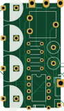
About the Buck-Boost converter simulation PCB
Buck-Boost converter simulation is an open source PCB design by abhishek-rath125, published on GitHub under the MIT license. It is a 2-layer board measuring 22.1 × 40 mm, with 16 components from 9 distinct parts.
Other key parts include the NE555P. By type, the board carries 4 capacitors, 4 resistors, 2 diodes, 2 inductors, 1 IC and 1 transistor.
It belongs with the power & battery designs in this gallery.
From the project
This directory contains the complete hardware design, schematic, 2-layer PCB layout, Bill of Materials (BOM), and manufacturing Gerber files for the Single-Stage Buck / Boost Demonstrator.
This directory contains the complete hardware design, schematic, 2-layer PCB layout, Bill of Materials (BOM), and manufacturing Gerber files for the Single-Stage Buck / Boost Demonstrator.
The hardware translates the dual-mode SEPIC / buck-boost topology into a physical board powered by a single supply and tuned in real time via an on-board trimmer potentiometer:
Main components on the Buck-Boost converter simulation
Buck-Boost converter simulation bill of materials (BOM)
16 components, 9 distinct parts — part numbers from the project's BOM.
| Qty | Part | Footprint | Refs |
|---|---|---|---|
| 1 | NE555P | DIP-8_W7.62mm | U1 |
| 1 | IRF3205 | TO-218-3_Vertical | Q1 |
| 1 | Conn_01x02_Pin | JWT_A3963_1x02_P3.96mm_Vertical | J1 |
| 1 | R_Potentiometer | Potentiometer_ACP_CA9-V10_Vertical | RV1 |
| 1 | D | D_DO-35_SOD27_P7.62mm_Horizontal | D1 |
| 1 | BAT54C | TO-126-3_Vertical | D3 |
| 2 | L | L_Axial_L11.0mm_D4.5mm_P7.62mm_Vertical_Fastron_MECC | L2, L3 |
| 4 | C_Small_US | CP_Radial_D10.0mm_P5.00mm | C2, C3, C4, C5 |
| 4 | R | R_Axial_DIN0204_L3.6mm_D1.6mm_P5.08mm_Horizontal | R1, R2, R3, R4 |
Buck-Boost converter simulation design files
The KiCad project lives in the abhishek-rath125/Buck-Boost-converter-simulation repository on GitHub; these links point at the commit this page was built from.
Buck-Boost converter simulation: common questions
How big is the Buck-Boost converter simulation PCB?
The Buck-Boost converter simulation measures 22.1 × 40 mm, has 2 copper layers and is 1.6 mm thick.
How many components are on the Buck-Boost converter simulation?
16 components, from 9 distinct parts, with part numbers taken from the project's own BOM. The full bill of materials is listed on this page.
Where can I download the Buck-Boost converter simulation design files?
From the abhishek-rath125/Buck-Boost-converter-simulation repository on GitHub, which has the KiCad layout, the schematic and the BOM; the links under Design files point to each one.
Can I use the Buck-Boost converter simulation design in my own project?
Yes, under the terms of its MIT license, which abhishek-rath125 chose for the repository.
Similar boards
EinkPDA screen
TalismanDesign
95 × 54 mm27 parts2LApache-2.02.0k
Stack chan
stack-chan
50 × 50 mm33 parts2LApache-2.01.7k
Display Carrier
AxxAxx
35.6 × 58.2 mm5 parts2LGPL-3.01.7k
ProgrammingAdapter
stuartpittaway
10.5 × 83 mm3 parts2LCC-BY-NC-4.01.1k
TemperaturePCB PANEL
116 × 75.5 mm178 parts2LCC-BY-NC-4.01.1k
Module 16S PassiveBalanceAddOn
61 × 74 mm86 parts2LCC-BY-NC-4.01.1k