
I2C Splitter

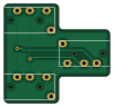
About the I2C Splitter PCB
I2C Splitter is an open source PCB design by Accessible-AAC, published on GitHub. It is a 2-layer board measuring 25.2 × 23.4 mm, with 3 components from 1 distinct parts.
From the project
Augmentative and alternative communications device design files based on inexpensive and open source technologies.
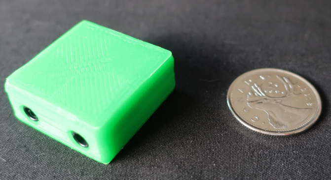
These directories contain design files for an i2c bus splitter, for use with an i2c (green) controller input.
This splitter can be used to connect two i2c (green base) peripherals to the same i2c (green) input port.
(Multiple splitters can be daisy-chained together to accommodate more i2c peripherals, subject to i2c bus limitation with respect to peripheral addressing.)
I2C Splitter bill of materials (BOM)
3 components, 1 distinct parts — part numbers from the project's BOM.
| Qty | Part | Footprint | Refs |
|---|---|---|---|
| 3 | PJ320A | PJ-320A | J1, J2, J3 |
I2C Splitter design files
The KiCad project lives in the Accessible-AAC/AAC-Devices repository on GitHub; these links point at the commit this page was built from.
I2C Splitter: common questions
How big is the I2C Splitter PCB?
The I2C Splitter measures 25.2 × 23.4 mm, has 2 copper layers and is 1.6 mm thick.
How many components are on the I2C Splitter?
3 components, from 1 distinct parts, with part numbers taken from the project's own BOM. The full bill of materials is listed on this page.
Where can I download the I2C Splitter design files?
From the Accessible-AAC/AAC-Devices repository on GitHub, which has the KiCad layout and the BOM; the links under Design files point to each one.
Can I use the I2C Splitter design in my own project?
The repository has no license, so all rights stay with Accessible-AAC. Use it as a reference, and ask the author before reusing the design.
More boards in AAC-Devices
 AVR/Arduino
Atmega32u4 hub pcb 1 3
71.9 × 58.4 mm65 parts2LNo license3 AVR/Arduino
Atmega32u4 hub pcb 1 2
71.9 × 58.4 mm65 parts2LNo license3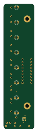
Tactile Switch Interface Board
26.4 × 108 mm22 parts2LNo license3
Arcade Joystick Interface Board
19.1 × 22.9 mm6 parts2LNo license3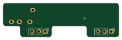
Dual Catalex Touch Sensor Interface Board
43.9 × 13 mm3 parts2LNo license3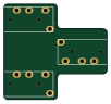
Switch Adaptor
25.2 × 23.4 mm3 parts2LNo license3