
Apple II Breakout

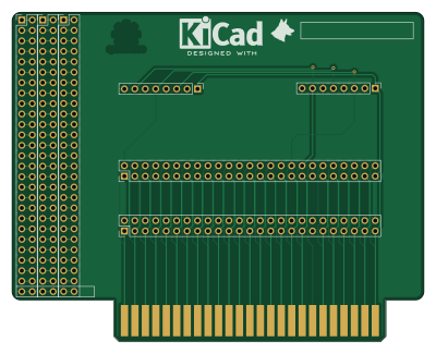
About the Apple II Breakout
Apple II Breakout is an open source PCB design by akuker, published on GitHub under the BSD-3-Clause license. It is a 2-layer board measuring 100 × 80 mm, with 8 components from 6 distinct parts.
It belongs with the dev boards & breakouts designs in this gallery.
Apple II Breakout bill of materials (BOM)
8 components, 6 distinct parts — part numbers from the project's BOM.
| Qty | Part | Footprint | Refs |
|---|---|---|---|
| 2 | Conn_01x08_Male | PinHeader_1x08_P2.54mm_Vertical | J1, J3 |
| 1 | Conn_02x25_Counter_Clockwise | PinHeader_2x25_P2.54mm_Vertical | J2 |
| 1 | U254-051N-4BH806 Conn_02x25_Counter_Clockwise | PinHeader_2x25_P2.54mm_Vertical | J4 |
| 1 | C2346 Conn_02x40_Top_Bottom | PinHeader_2x27_P2.54mm_Vertical | J5 |
| 2 | Conn_02x40_Top_Bottom | PinHeader_2x27_P2.54mm_Vertical | J6, J7 |
| 1 | A2_BUS | BUS_A2 | BUS1 |
Apple II Breakout design files
The KiCad project lives in the akuker/hw_projects repository on GitHub; these links point at the commit this page was built from.
Apple II Breakout: common questions
How big is the Apple II Breakout?
The Apple II Breakout measures 100 × 80 mm, has 2 copper layers and is 1.6 mm thick.
How many components are on the Apple II Breakout?
8 components, from 6 distinct parts, with part numbers taken from the project's own BOM. The full bill of materials is listed on this page.
Where can I download the Apple II Breakout design files?
From the akuker/hw_projects repository on GitHub, which has the KiCad layout and the BOM; the links under Design files point to each one.
Can I use the Apple II Breakout design in my own project?
Yes, under the terms of its BSD-3-Clause license, which akuker chose for the repository.
More boards in hw_projects
Pixel grid
51.3 × 51.6 mm303 parts4LBSD-3-Clause2 RP2040/RP2350
VintageKVM
200 × 73.6 mm120 parts2LBSD-3-Clause2 RP2040/RP2350
Scsi switcher
160 × 100 mm75 parts4LBSD-3-Clause2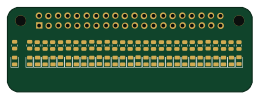
Rpi led board
65 × 22.4 mm59 parts2LBSD-3-Clause2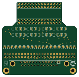
Daisy chain board
65 × 63.1 mm56 parts2LBSD-3-Clause2 STM32
STM32Stm8 breakout board
21.8 × 26.9 mm23 parts2LBSD-3-Clause2 WCH CH32/CH55x
Ch554 USB Host Test
55.1 × 19 mm19 parts2LBSD-3-Clause2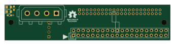
Ata 40 to ata 44 adapter
86 × 18.5 mm8 parts2LBSD-3-Clause2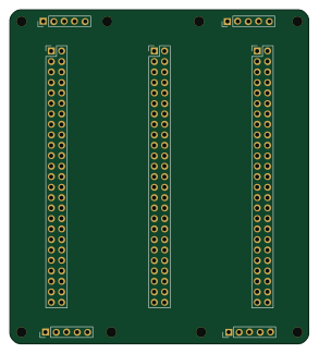
Fifty pin header breakout
72.5 × 81 mm7 parts2LBSD-3-Clause2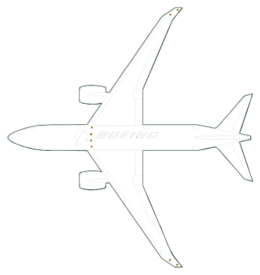
787
92.3 × 97.8 mm4 parts2LBSD-3-Clause2
Similar boards
Radioberry juice
pa3gsb
65 × 56 mm87 parts2LNo license675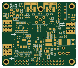
Radioberry preamp
65 × 56 mm137 parts2LNo license675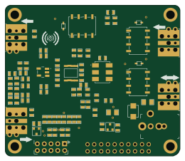
Hat
65 × 56 mm81 parts2LNo license675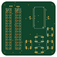
Sram dev board
Wren6991
50 × 50 mm12 parts2LNo license508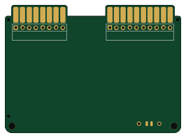
ESP32
Chrismettal
66.4 × 48.1 mm20 parts2LCC-BY-SA-4.0446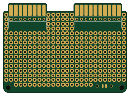
ESP32
66.4 × 48.1 mm20 parts2LCC-BY-SA-4.0446