
Boost Electrical Draft

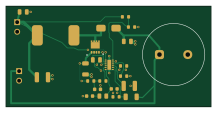
About the Boost Electrical Draft PCB
Boost Electrical Draft is an open source PCB design by AnishLanka, published on GitHub. It is a 2-layer board measuring 54.2 × 26.5 mm, with 25 components from 25 distinct parts.
Other key parts include the LM5155DSSR. By type, the board carries 10 resistors, 9 capacitors, 2 connectors, 1 IC, 1 transistor and 1 diode.
From the project
79.7 V BOOST - ENGINEERING BENCH PROTOTYPE
79.7 V BOOST - ENGINEERING BENCH PROTOTYPE
Open BoostElectricalDraft.kicadpro in KiCad10. The schematic, PCB and local libraries are included. The routed PCB matches the schematic and passes the checks in PCBDRC.json / PCBValidation.json. Read PCBDraftNotes.txt for mechanics, pinout and layout decisions, DraftReview.txt for electrical assumptions, and FabricationOrderNotes.txt for the0.4 mm bare-board order. The top-level upload archive is Boost79V7Prototype_JLCPCB.zip. The hardware still requires assembly and bench testing.
Main components on the Boost Electrical Draft
Boost Electrical Draft bill of materials (BOM)
25 components, 25 distinct parts — part numbers from the project's BOM.
| Qty | Part | Footprint | Refs |
|---|---|---|---|
| 1 | LM5155DSSR Texas Instruments | U1_DSS0012B | U1 |
| 1 | FDMC86240 onsemi | Q_FDMC86240_CASE511DH | Q1 |
| 1 | 12V INPUT | IN_FP-TSW-102-14-G-S-MFG | J1 |
| 1 | 80V OUTPUT | OUT_FP-TSW-102-14-G-S-MFG | J2 |
| 1 | SS120 SS120 200V Taiwan Semiconductor | D_SMA | D1 |
| 1 | SRR1280-102K 1mH SRR1280-102K Bourns | L_BOURNS | L1 |
| 1 | C2012X5R1H106K125AC 10u 50V TDK | C0805 | C1 |
| 1 | C1608C0G1H680J080AA 68p 50V TDK | C0603 | C2 |
| 1 | C1608X7R1H473K080AA 47n 50V TDK | C0603 | C3 |
| 1 | C2012X7R1E225K125AB 2.2u 25V TDK | C0805 | C4 |
| 1 | EEUEE2C101S 100u 160V Panasonic | C_BULK | C5 |
| 1 | C1608C0G1H101J080AA 100p 50V TDK | C0603 | C6 |
| 1 | GRM32ER61C476KE15L 47u 16V Murata | C1210 | C7 |
| 1 | C2012X7T2E104K125AA 100n 250V TDK | C0805 | C8 |
| 1 | MSAST32MAB5476MPNDT1 47u 25V Taiyo Yuden | C1210 | C9 |
| 1 | TNPW1206787KBEEA 787k 0.1% Vishay | R1206 | R1 |
| 1 | TNPW060310K0BEEA 10k 0.1% Vishay | R0603 | R2 |
| 1 | CRCW060354K9FKEA 54.9k 1% Vishay | R0603 | R3 |
| 1 | CRCW0603100RFKEA 100R 1% Vishay | R0603 | R4 |
| 1 | CRCW0603909RFKEA 909R 1% Vishay | R0603 | R5 |
Show 5 more
| Qty | Part | Footprint | Refs |
|---|---|---|---|
| 1 | CRCW0603110KFKEA 110k 1% Vishay | R0603 | R6 |
| 1 | CRCW060324K9FKEA 24.9k 1% Vishay | R0603 | R7 |
| 1 | CRCW0805191KFKEA 191k 1% Vishay | R0805 | R8 |
| 1 | ERJ8BQFR27V 0R270 1% Panasonic | R1206 | R9 |
| 1 | CRCW060321K5FKEA 21.5k 1% Vishay | R0603 | R10 |
Boost Electrical Draft design files
The KiCad project lives in the AnishLanka/BrainStimulation repository on GitHub; these links point at the commit this page was built from.
Boost Electrical Draft: common questions
How big is the Boost Electrical Draft PCB?
The Boost Electrical Draft measures 54.2 × 26.5 mm, has 2 copper layers and is 0.41116 mm thick.
How many components are on the Boost Electrical Draft?
25 components, from 25 distinct parts, with part numbers taken from the project's own BOM. The full bill of materials is listed on this page.
Where can I download the Boost Electrical Draft design files?
From the AnishLanka/BrainStimulation repository on GitHub, which has the KiCad layout, the schematic and the BOM; the links under Design files point to each one.
Can I use the Boost Electrical Draft design in my own project?
The repository has no license, so all rights stay with AnishLanka. Use it as a reference, and ask the author before reusing the design.
More boards in BrainStimulation
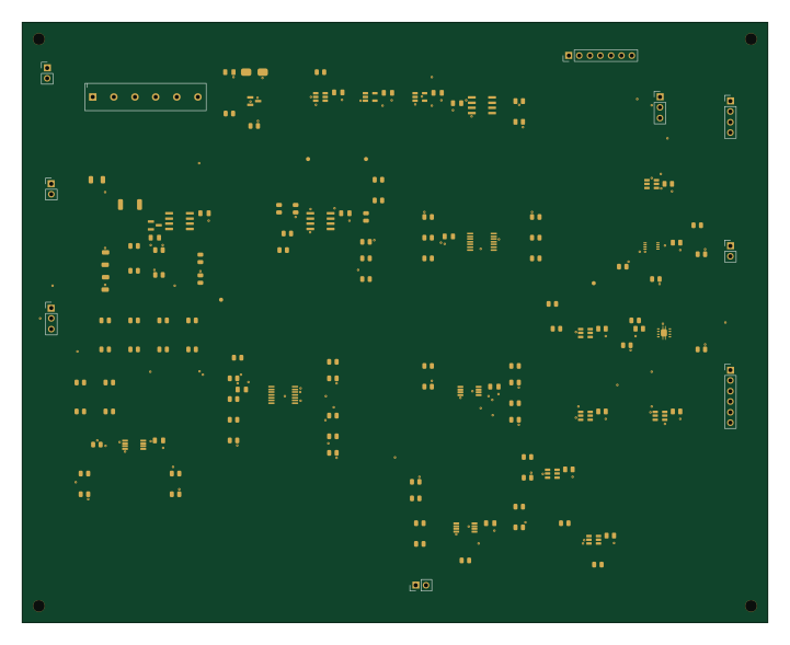
Channel Monitor C1
180 × 145 mm137 parts2LNo license1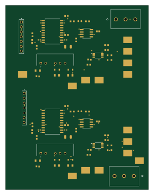
SignalGen Electrical Draft
74.7 × 95.9 mm77 parts2LNo license1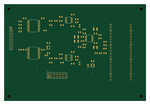 RP2040/RP2350
Channel ADC Interface RevC
125 × 85 mm69 parts2LNo license1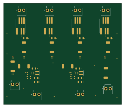
Shared regulated 5V power adapter
105 × 90 mm40 parts2LNo license1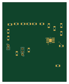
HowlandPump-AnishWork
56 × 70 mm19 parts2LNo license1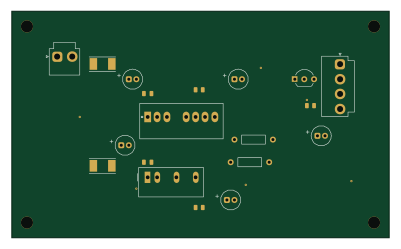
Monitor Power C1
100 × 60 mm19 parts2LNo license1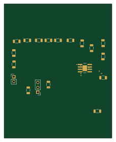
HowlandPump-AnishWorkFINAL
56 × 70 mm19 parts2LNo license1
HowlandPump-AnishWorkBackout
56 × 70 mm19 parts2LNo license1
RailSplitter Electrical Draft
50.7 × 19.4 mm12 parts2LNo license1
BuckBoost RevB
58.9 × 17 mm9 parts2LNo license1