
SignalGen Electrical Draft

About the SignalGen Electrical Draft PCB
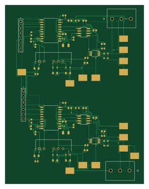
SignalGen Electrical Draft is an open source PCB design by AnishLanka, published on GitHub. It is a 2-layer board measuring 74.7 × 95.9 mm, with 77 components from 70 distinct parts.
Other key parts include the ISOW7741DFM, DAC8830IBD and OPA2192IDGKR. By type, the board carries 42 capacitors, 15 test points, 8 resistors, 6 ICs and 4 connectors.
It belongs with the power & battery and test & measurement designs in this gallery.
From the project
By Pythagoras Carayannopoulos, Peter Zhao and Anish Lanka. Presentation: docs/PrototypeDemo2.pdf
By Pythagoras Carayannopoulos, Peter Zhao and Anish Lanka. Presentation: docs/PrototypeDemo2.pdf
Start with docs/RevCRelease/READMEFIRST.txt and docs/RevCRelease/IntegrationGuide.html`. Upload each board's manufacturing ZIP to JLCPCB as a separate bare PCB design. Do not upload the complete release archive as one PCB.
The signal generator sets the shape of the stimulation current. The power path provides the energy and voltage to push it. The two paths meet at the Howland, which turns the voltage command into a current.
Main components on the SignalGen Electrical Draft
SignalGen Electrical Draft bill of materials (BOM)
77 components, 70 distinct parts — part numbers from the project's BOM.
| Qty | Part | Footprint | Refs |
|---|---|---|---|
| 1 | ISOW7741DFM Texas Instruments | U1_SOIC20_DFM_TEX | U1 |
| 2 | DAC8830IBD | SOIC-8_3.9x4.9mm_P1.27mm | U3, U5 |
| 1 | OPA2192IDGKR | U4_DGK0008A_N_TEX | U4 |
| 1 | ISOW7741DFM | U6_SOIC20_DFM_TEX | U6 |
| 1 | OPA2192IDGKR | U7_DGK0008A_N_TEX | U7 |
| 1 | TSW-102-14-G-S SS-107-T-1A Samtec | J1_SAMTEC_SS-107-T-1A | J1 |
| 1 | TSW-102-14-G-S SS-107-T-1A Samtec | J2_SAMTEC_SS-107-T-1A | J2 |
| 1 | 1716030000 | J3_CONN_LM_5.080390_WED | J3 |
| 1 | 1716030000 | J4_CONN_LM_5.080390_WED | J4 |
| 1 | IA0305S | PS1_XP_IA0305S | PS1 |
| 1 | IA0305S | PS2_XP_IA0305S | PS2 |
| 1 | +ISO_P5V | TP1_KEYSTONE_5016 | TP1 |
| 1 | -ISO_N5V | TP2_KEYSTONE_5016 | TP2 |
| 1 | ISO_GND_ISOW | TP3_KEYSTONE_5016 | TP3 |
| 1 | Bi_PolarOut | TP6_KEYSTONE_5016 | TP6 |
| 1 | VREF_BUF_TP | TP7_KEYSTONE_5016 | TP7 |
| 1 | TP_SYS_3V3 | TP8_KEYSTONE_5016 | TP8 |
| 1 | TP_ISO_3V3_CLEAN | TP9_KEYSTONE_5016 | TP9 |
| 1 | TP_ISO_3V3_RAW | TP10_KEYSTONE_5016 | TP10 |
| 1 | TP_ISO_3V3_CLEAN_2 | TP11_KEYSTONE_5016 | TP11 |
Show 50 more
| Qty | Part | Footprint | Refs |
|---|---|---|---|
| 1 | TP_ISO_3V3_RAW_2 | TP12_KEYSTONE_5016 | TP12 |
| 1 | +ISO_P5V_2 | TP13_KEYSTONE_5016 | TP13 |
| 1 | -ISO_N5V_2 | TP14_KEYSTONE_5016 | TP14 |
| 1 | ISO_GND_ISOW_2 | TP15_KEYSTONE_5016 | TP15 |
| 1 | Bi_PolarOut_2 | TP16_KEYSTONE_5016 | TP16 |
| 1 | VREF_BUF_TP_2 | TP17_KEYSTONE_5016 | TP17 |
| 1 | GRM21BR61E106KA73L 10uF TDK | C1_G-21_MUR | C1 |
| 1 | CC0603KRX7R8BB104 100nF TDK | C2_CAPC1608X90N | C2 |
| 1 | CC0603KRX7R8BB104 100nF SYS TDK | C3_CAPC1608X90N | C3 |
| 1 | MBASE168SB7105KTNA18 1uF TDK | C4_INDC1608X90N | C4 |
| 1 | MBASE168SB7105KTNA18 1uF Panasonic | C5_INDC1608X90N | C5 |
| 1 | CC0603KRX7R8BB104 100nF ISO TDK | C6_CAPC1608X90N | C6 |
| 1 | MBASE168SB7105KTNA18 1uF TDK | C8_INDC1608X90N | C8 |
| 1 | MBASE168SB7105KTNA18 1uF Taiyo Yuden | C9_INDC1608X90N | C9 |
| 1 | CC0603KRX7R8BB104 100nF | C10_CAPC1608X90N | C10 |
| 1 | C1608X7R1H474K080AC 470nF | C12_CAP_1608_TDK | C12 |
| 1 | C1608X7R1H474K080AC 470nF | C13_CAP_1608_TDK | C13 |
| 1 | GRM21BR61E106KA73L 10uF | C14_G-21_MUR | C14 |
| 1 | GRM21BR61E106KA73L 10uF | C15_G-21_MUR | C15 |
| 1 | CC0603KRX7R8BB104 100nF | C17_CAPC1608X90N | C17 |
| 1 | CC0603KRX7R8BB104 100nF | C18_CAPC1608X90N | C18 |
| 1 | MBASE168SB7105KTNA18 1uF | C19_INDC1608X90N | C19 |
| 1 | MBASE168SB7105KTNA18 1uF | C20_INDC1608X90N | C20 |
| 1 | MBASE168SB7105KTNA18 1uF | C21_INDC1608X90N | C21 |
| 1 | MBASE168SB7105KTNA18 1uF | C22_INDC1608X90N | C22 |
| 1 | CC0603KRX7R8BB104 100nF | C23_CAPC1608X90N | C23 |
| 1 | MBASE168SB7105KTNA18 1uF | C24_INDC1608X90N | C24 |
| 1 | MBASE168SB7105KTNA18 1uF | C25_INDC1608X90N | C25 |
| 1 | CC0603KRX7R8BB104 100nF ISO_2 | C26_CAPC1608X90N | C26 |
| 1 | CC0603KRX7R8BB104 100nF SYS | C27_CAPC1608X90N | C27 |
| 1 | GRM21BR61E106KA73L 10uF | C28_G-21_MUR | C28 |
| 1 | GRM21BR61E106KA73L 10uF | C29_G-21_MUR | C29 |
| 1 | C1608X7R1H474K080AC 470nF | C30_CAP_1608_TDK | C30 |
| 1 | C1608X7R1H474K080AC 470nF | C31_CAP_1608_TDK | C31 |
| 1 | CC0603KRX7R8BB104 100nF | C33_CAPC1608X90N | C33 |
| 1 | CC0603KRX7R8BB104 100nF | C34_CAPC1608X90N | C34 |
| 1 | MBASE168SB7105KTNA18 1uF | C35_INDC1608X90N | C35 |
| 1 | MBASE168SB7105KTNA18 1uF | C36_INDC1608X90N | C36 |
| 1 | MBASE168SB7105KTNA18 1uF | C37_INDC1608X90N | C37 |
| 1 | MBASE168SB7105KTNA18 1uF | C38_INDC1608X90N | C38 |
| 1 | GRM21BR61E106KA73L 10uF | C39_G-21_MUR | C39 |
| 1 | CC0603KRX7R8BB104 100nF | C40_CAPC1608X90N | C40 |
| 2 | TBD - draft value/footprint only 22u | C_1206_3216Metric | C41, C44 |
| 4 | TBD - draft value/footprint only 10n | C_0402_1005Metric | C42, C43, C45, C46 |
| 1 | RC0603FR-0720KL 20K Vishay | R3_RC0603N_YAG | R3 |
| 1 | RC0603FR-0720KL 20K Vishay | R6_RC0603N_YAG | R6 |
| 1 | RC0603FR-0720KL 20K | R11_RC0603N_YAG | R11 |
| 1 | RC0603FR-0720KL 20K | R12_RC0603N_YAG | R12 |
| 2 | RC0603FR-0710KL 10K | R_0603_1608Metric | R13, R14 |
| 2 | TBD - standard 0603 zero-ohm jumper 0 | R_0603_1608Metric | R15, R16 |
SignalGen Electrical Draft design files
The KiCad project lives in the AnishLanka/BrainStimulation repository on GitHub; these links point at the commit this page was built from.
SignalGen Electrical Draft: common questions
How big is the SignalGen Electrical Draft PCB?
The SignalGen Electrical Draft measures 74.7 × 95.9 mm, has 2 copper layers and is 0.41116 mm thick.
How many components are on the SignalGen Electrical Draft?
77 components, from 70 distinct parts, with part numbers taken from the project's own BOM. The full bill of materials is listed on this page.
Where can I download the SignalGen Electrical Draft design files?
From the AnishLanka/BrainStimulation repository on GitHub, which has the KiCad layout, the schematic and the BOM; the links under Design files point to each one.
Can I use the SignalGen Electrical Draft design in my own project?
The repository has no license, so all rights stay with AnishLanka. Use it as a reference, and ask the author before reusing the design.
More boards in BrainStimulation
Channel Monitor C1
180 × 145 mm137 parts2LNo license1 RP2040/RP2350
Channel ADC Interface RevC
125 × 85 mm69 parts2LNo license1
Shared regulated 5V power adapter
105 × 90 mm40 parts2LNo license1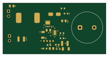
Boost Electrical Draft
54.2 × 26.5 mm25 parts2LNo license1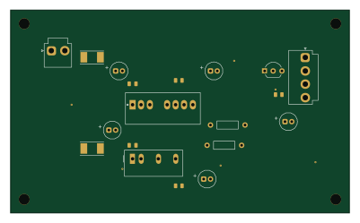
Monitor Power C1
100 × 60 mm19 parts2LNo license1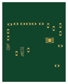
HowlandPump-AnishWorkBackout
56 × 70 mm19 parts2LNo license1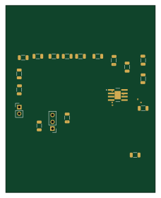
HowlandPump-AnishWork
56 × 70 mm19 parts2LNo license1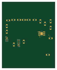
HowlandPump-AnishWorkFINAL
56 × 70 mm19 parts2LNo license1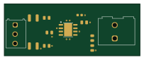
RailSplitter Electrical Draft
50.7 × 19.4 mm12 parts2LNo license1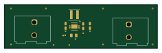
BuckBoost RevB
58.9 × 17 mm9 parts2LNo license1
Similar boards
StackLink
gusmanb
52.3 × 10.5 mm5 parts2LGPL-3.05.0k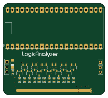
AnalyzerBoxPCB fork
52.7 × 47.9 mm54 parts4LGPL-3.05.0k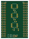
LevelShifter
28.3 × 39.8 mm21 parts2LGPL-3.05.0k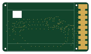
EinkPDA screen
TalismanDesign
95 × 54 mm27 parts2LApache-2.02.0k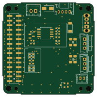
Stack chan
stack-chan
50 × 50 mm33 parts2LApache-2.01.7k
Display Carrier
AxxAxx
35.6 × 58.2 mm5 parts2LGPL-3.01.7k