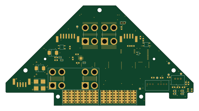
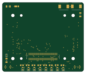
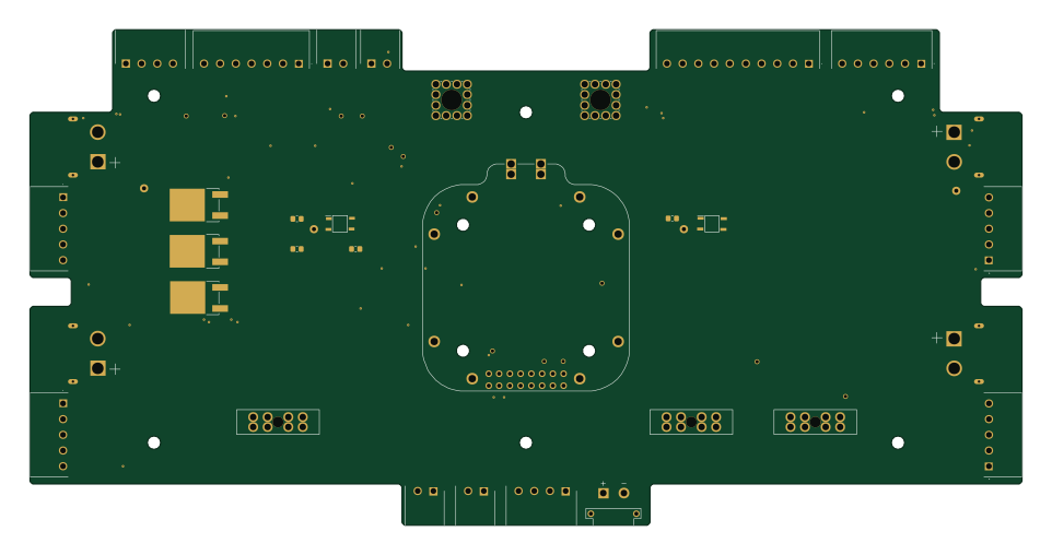
Quiver PT3 Main PCB-rounded

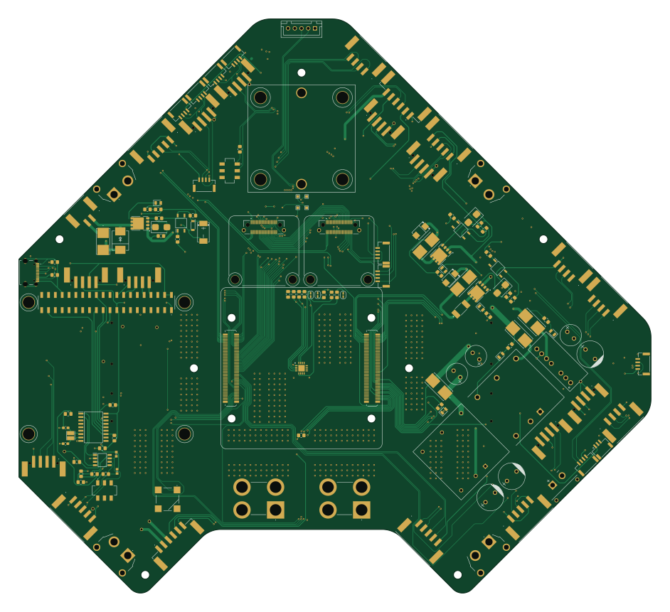
About the Quiver PT3 Main PCB-rounded
Quiver PT3 Main PCB-rounded is an open source PCB design by Arrow-air, published on GitHub under the CERN-OHL-S-2.0 license. It is a 6-layer board measuring 235.1 × 213.7 mm, with 157 components from 64 distinct parts.
Other key parts include the TSYS01, TJA1049T/3J, MCP2515-I/SO, SMTSOM380BTR and URB4805S-6WR3. By type, the board carries 54 connectors, 33 resistors, 19 capacitors, 17 ICs, 8 diodes and 7 fuses.
From the project
Project Quiver documentation, designs, and project artifacts.
KiCad projects for the Quiver's distributed PCB architecture.
Production gerbers live in each project's production/ folder. Design history, update notes, and superseded board revisions remain with the bounty tasks under task-grant-bounty/pt3/electronics/.
Each KiCad project can export a 3D STEP model of the assembled board. These STEP files go into the CAD assembly tree:
Main components on the Quiver PT3 Main PCB-rounded
Quiver PT3 Main PCB-rounded bill of materials (BOM)
157 components, 64 distinct parts — part numbers from the project's BOM.
| Qty | Part | Footprint | Refs |
|---|---|---|---|
| 1 | TSYS01 | QFN65P400X400X90-17N | IC1 |
| 1 | TJA1049T/3J NXP | SOIC127P600X175-8N | U1 |
| 1 | MCP2515-I/SO Microchip | SOIC127P1030X265-18N | U2 |
| 4 | SMTSOM380BTR YIYUAN(怡远) | SMD_BD6.0-D4.2 | U3, U6, U7, U8 |
| 1 | URB4805S-6WR3 YLPTEC(易川) | PWRM-TH_YLPTEC_URBXXXXS-6WR3 | U4 |
| 1 | 1814935 C7429635 Megastar(兆星) | CONN-TH_5P-P2.50_ZX-XH2.54-5PZZ | U5 |
| 4 | SMTSO25100CTJ Sinhoo(雄和远景) | SMD_BD5.6-L5.6-W5.6-D4.1 | U9, U10, U11, U12 |
| 4 | SMTWEM245STR YIYUAN(怡远) | SCREW-SMD_BD4.4-D2.8-H4.5 | U13, U14, U15, U16 |
| 2 | SIR804DP-T1-GE3 SIRA99DP-T1-GE3 VISHAY(威世) | POWERPAK-SO-8_L5.9-W4.9-P1.27-LS6.2-BL | Q1, Q2 |
| 1 | SIR804DP-T1-GE3 SIR570DP-T1-RE3 VISHAY(威世) | POWERPAK-SO-8_L5.9-W4.9-P1.27-LS6.2-BL | Q3 |
| 1 | NX3225GB-16M-STD-CRA-2 16MHz NDK | NX3225GB-16M-STD-CRA-2 | X1 |
| 1 | SSQ-120-01-F-D RPI_5_WITH_SSQ-120-01-F-D | SSM-120-XXX-DV | J1 |
| 11 | 1778719 | 1778719 | J2, J6, J10, J12, J13, J16, J19, J21 +3 |
| 2 | AXK5S00347YG AXK6S00547YG | AXK6S00547YG | J3, J4 |
| 11 | SM04B-GHS-TB(LF)(SN) SM04B-GHS-TB_LF__SN_ | SM04B-GHS-TB | J5, J7, J9, J15, J18, J20, J22, J35 +3 |
| 5 | 1814935 | 1814935 | J8, J39, J49, J50, J53 |
| 1 | SSQ-104-01-L-D M9N-G4-3100 | M9N-G4-3100 | J11 |
| 1 | XT30PW-F | XT30PW-F_AMASS_XT30PW-F | J14 |
| 1 | 1814922 SM03B-GHS-TB(LF)(SN) JST | CONN-TH_SM03B-GHS-TB-LF-SN | J17 |
| 5 | 1814948 | 1814948 | J23, J27, J32, J40, J43 |
Show 44 more
| Qty | Part | Footprint | Refs |
|---|---|---|---|
| 4 | XT60PW-F | XT60PWF | J25, J28, J34, J42 |
| 1 | 1814919 | 1814919 | J26 |
| 2 | 1778735 | 1778735 | J29, J30 |
| 2 | 1814951 | 1814951 | J31, J46 |
| 1 | USB4216-03-A | USB421603A | J33 |
| 1 | SM05B-GHS-TB(LF)(SN) SM05B-GHS-TB_LF__SN_ | SM05B-GHS-TB | J36 |
| 1 | SM06B-GHS-TB(LF)(SN) SM06B-GHS-TB_LF__SN_ | SM06B-GHS-TB | J41 |
| 2 | AMT0450003DB0000G | AMT0450003DB0000G | J44, J45 |
| 2 | LSHM-120-02.5-L-DV-A-S-K-TR GIGABLOX_NANO_SWITCH_REVA_MODULE | GIGABLOX_NANO_SWITCH_REVA_MODULE_LSHM-120-02.5-L-DV-A-S-K-TR | J47, J51 |
| 2 | 0154002.DR | 0154002DR | F1, F7 |
| 3 | 0154005.DR | 0154005DR | F2, F3, F4 |
| 1 | 0154001.DR | 0154001DR | F5 |
| 1 | 1812L110/24DR 1812L110_24DR | 1812L010DR | F8 |
| 3 | CPC1019N | SOP254P610X218-4N | K1, K2, K3 |
| 1 | CMT-8530S-SMT-TR | CMT8530SSMTTR | LS1 |
| 1 | REC20K-4805SZ | REC20K | PS1 |
| 1 | REC30K-4812SZ | REC30K | PS2 |
| 2 | SLW-913535-2A-SMT CUI Devices | SLW9135352ASMT | S1, S2 |
| 1 | MMSZ5242B-E3-08 | SOD3716X135N | Z1 |
| 6 | APT2012LVBC/D APT2012LVBC_D | LEDC2012X85N | LED1, LED2, LED3, LED4, LED5, LED6 |
| 2 | PESD0603-240 LITTELFUSE | DIONC1608X55N | D1, D2 |
| 3 | SMBJ13CA hongjiacheng | D_SMB | D3, D4, D5 |
| 2 | SS34 BORN(伯恩半导体) | SMB_L4.6-W3.6-LS5.3-RD | D6, D7 |
| 1 | ES3D onsemi(安森美) | SMC_L7.1-W6.2-LS8.1-RD | D8 |
| 4 | CC0805KRX7R9BB104 100nF Yageo | C_0805_2012Metric_Pad1.18x1.45mm_HandSolder | C1, C3, C4, C5 |
| 3 | 100UF 100uF NJCON(永立) | CAP-TH_BD10.0-P5.00-D0.6-FD_2 | C2, C8, C11 |
| 2 | CC0603JRNPO9BN8R0 8pF Yageo | C_0603_1608Metric_Pad1.08x0.95mm_HandSolder | C6, C7 |
| 3 | 470UF 470uF Yunxing(云星) | CAP-TH_BD8.0-P3.50-D0.6-FD | C9, C10, C12 |
| 6 | 1UF 1uF SAMSUNG(三星) | C1206 | C13, C14, C15, C16, C17, C18 |
| 1 | 22UF 22uF PANASONIC(松下) | CAP-SMD_L7.3-W4.3-RD_PA300LV227M0J | C19 |
| 3 | 1K5 | R_0805_2012Metric_Pad1.20x1.40mm_HandSolder | R1, R27, R28 |
| 4 | 100K 100k | R_0805_2012Metric_Pad1.20x1.40mm_HandSolder | R2, R4, R5, R26 |
| 3 | 100R | R_0805_2012Metric_Pad1.20x1.40mm_HandSolder | R3, R6, R22 |
| 2 | 10K | R_0805_2012Metric_Pad1.20x1.40mm_HandSolder | R7, R9 |
| 1 | RC0805FR-0710KL 100k Yageo | R_0805_2012Metric_Pad1.20x1.40mm_HandSolder | R8 |
| 6 | RC0805FR-0710KL 10K Yageo | R_0805_2012Metric_Pad1.20x1.40mm_HandSolder | R10, R11, R17, R19, R20, R21 |
| 2 | 5K1 | R_0805_2012Metric_Pad1.20x1.40mm_HandSolder | R12, R13 |
| 2 | RC0805FR-07120RL 120R Yageo | R_0805_2012Metric_Pad1.20x1.40mm_HandSolder | R14, R18 |
| 1 | 47K | R_0805_2012Metric_Pad1.20x1.40mm_HandSolder | R15 |
| 1 | RC0805FR-070RL 0R Yageo | R_0805_2012Metric_Pad1.20x1.40mm_HandSolder | R16 |
| 2 | 1K2 | R_0805_2012Metric_Pad1.20x1.40mm_HandSolder | R23, R24 |
| 3 | 4K7 | R_0805_2012Metric_Pad1.20x1.40mm_HandSolder | R25, R29, R30 |
| 2 | 15K | R_0805_2012Metric_Pad1.20x1.40mm_HandSolder | R31, R32 |
| 1 | 0R | R_0805_2012Metric_Pad1.20x1.40mm_HandSolder | R33 |
Quiver PT3 Main PCB-rounded design files
The KiCad project lives in the Arrow-air/project-quiver repository on GitHub; these links point at the commit this page was built from.
Quiver PT3 Main PCB-rounded: common questions
How big is the Quiver PT3 Main PCB-rounded?
The Quiver PT3 Main PCB-rounded measures 235.1 × 213.7 mm, has 6 copper layers and is 1.6 mm thick.
How many components are on the Quiver PT3 Main PCB-rounded?
157 components, from 64 distinct parts, with part numbers taken from the project's own BOM. The full bill of materials is listed on this page.
Where can I download the Quiver PT3 Main PCB-rounded design files?
From the Arrow-air/project-quiver repository on GitHub, which has the KiCad layout, the schematic and the BOM; the links under Design files point to each one.
Can I use the Quiver PT3 Main PCB-rounded design in my own project?
Yes, under the terms of its CERN-OHL-S-2.0 license, which Arrow-air chose for the repository.