
My keyboard

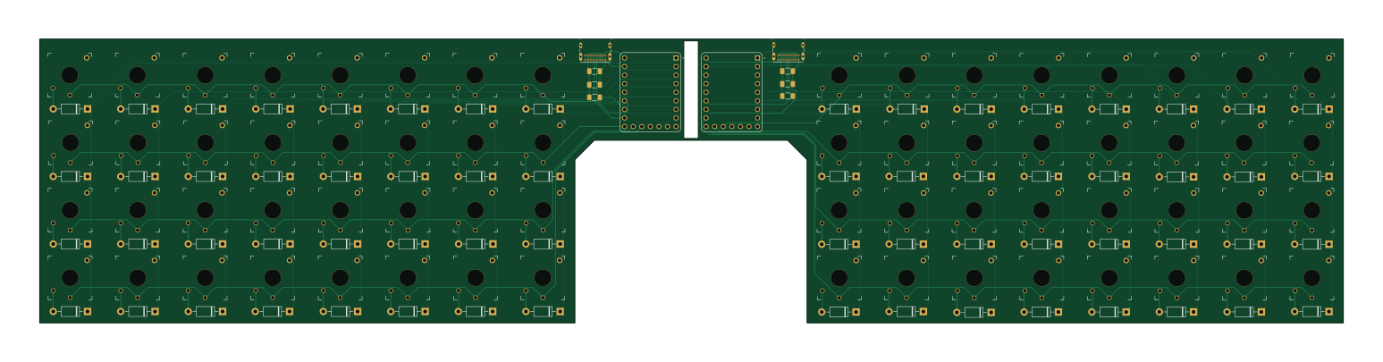
About the My keyboard PCB
My keyboard is an open source RP2040/RP2350 PCB design by Axel-Jacobsen, published on GitHub. It is a 2-layer board measuring 386.1 × 84.1 mm, with 138 components from 8 distinct parts.
Its main chip is the RP2040-ZERO, from the RP2040/RP2350 family. By type, the board carries 64 switches, 64 diodes, 4 capacitors, 2 ICs, 2 connectors and 2 resistors.
It belongs with the keyboards and dev boards & breakouts designs in this gallery.
From the project
dont worry bout this keyboard
split keyboard, fun to make and fun to have
TODOs ===== [ ] swap to low profile keys [ ] expose scl, sda [ ] tighten up PCB
microcontroller =============== - connection type - wired - pros: no battery, simpler, would be fun to program bluetooth controller - cons: annoying while using - bluetooth: - pros: clean to use - cons: battery is annoying - decision - wired to start[0] - bluetooth will make the project more complicated than necessary - possible options - ATmega32U4 (widely used, looks small) - as raw IC mounted on the PCB (more complicated, so don't do) or as a "hat" on a breakout…
Main components on the My keyboard
My keyboard bill of materials (BOM)
138 components, 8 distinct parts.
| Qty | Part | Footprint | Refs |
|---|---|---|---|
| 2 | RP2040-ZERO | MODULE_RP2040-ZERO | U1, U2 |
| 1 | L to R | USB_C_Receptacle_GCT_USB4085 | P1 |
| 1 | R to L | USB_C_Receptacle_GCT_USB4085 | P2 |
| 64 | SW_SPST | SW_Kailh_Choc_V2_THT | SW1, SW2, SW3, SW4, SW5, SW6, SW7, SW8 +56 |
| 64 | 1N5817 | D_DO-41_SOD81_P10.16mm_Horizontal | D1, D2, D3, D4, D5, D6, D7, D8 +56 |
| 2 | 100nF | C_1206_3216Metric_Pad1.33x1.80mm_HandSolder | C1, C3 |
| 2 | 10µF | C_1206_3216Metric_Pad1.33x1.80mm_HandSolder | C2, C4 |
| 2 | 4700 | R_1206_3216Metric_Pad1.30x1.75mm_HandSolder | R1, R2 |
My keyboard design files
The KiCad project lives in the Axel-Jacobsen/my-keyboard repository on GitHub; these links point at the commit this page was built from.
- Layoutpcb/pcb.kicad_pcb
- Schematicpcb/pcb.kicad_sch
My keyboard: common questions
What microcontroller does the My keyboard use?
The My keyboard is built around the RP2040-ZERO, from the RP2040/RP2350 family.
How big is the My keyboard PCB?
The My keyboard measures 386.1 × 84.1 mm, has 2 copper layers and is 1.6 mm thick.
How many components are on the My keyboard?
138 components, from 8 distinct parts. The full bill of materials is listed on this page.
Where can I download the My keyboard design files?
From the Axel-Jacobsen/my-keyboard repository on GitHub, which has the KiCad layout and the schematic; the links under Design files point to each one.
Can I use the My keyboard design in my own project?
The repository has no license, so all rights stay with Axel-Jacobsen. Use it as a reference, and ask the author before reusing the design.
Can I test firmware for the My keyboard without the hardware?
Yes. HardLabs builds a simulation of the board from its netlist and BOM, so you can run and debug RP2040/RP2350 firmware against it before you order a PCB.
Similar boards
 RP2040/RP2350
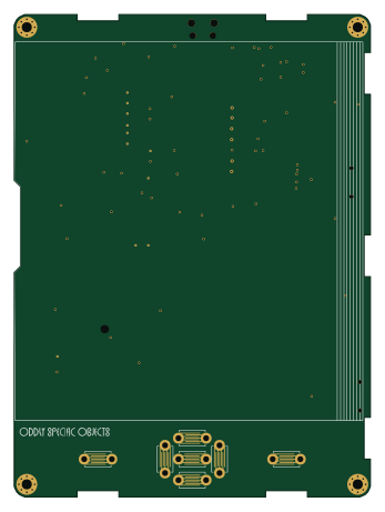
Open Book Abridged Edition
joeycastillo
85 × 115 mm29 parts2LCC-BY-SA-4.08.1k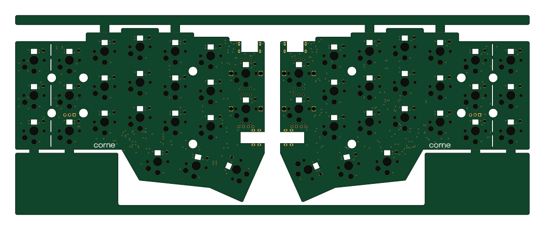 RP2040/RP2350
Corne
foostan
277.2 × 107.5 mm164 parts2LCC-BY-4.07.7k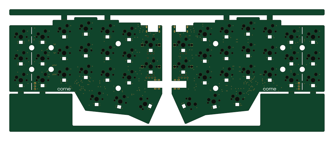 RP2040/RP2350
Corne
277.2 × 107.5 mm164 parts2LCC-BY-4.07.7k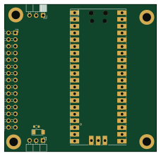 RP2040/RP2350
LogicAnalyzer
gusmanb
57 × 55.2 mm6 parts2LGPL-3.05.0k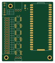 RP2040/RP2350
Jitx design
55.5 × 65 mm26 parts4LGPL-3.05.0k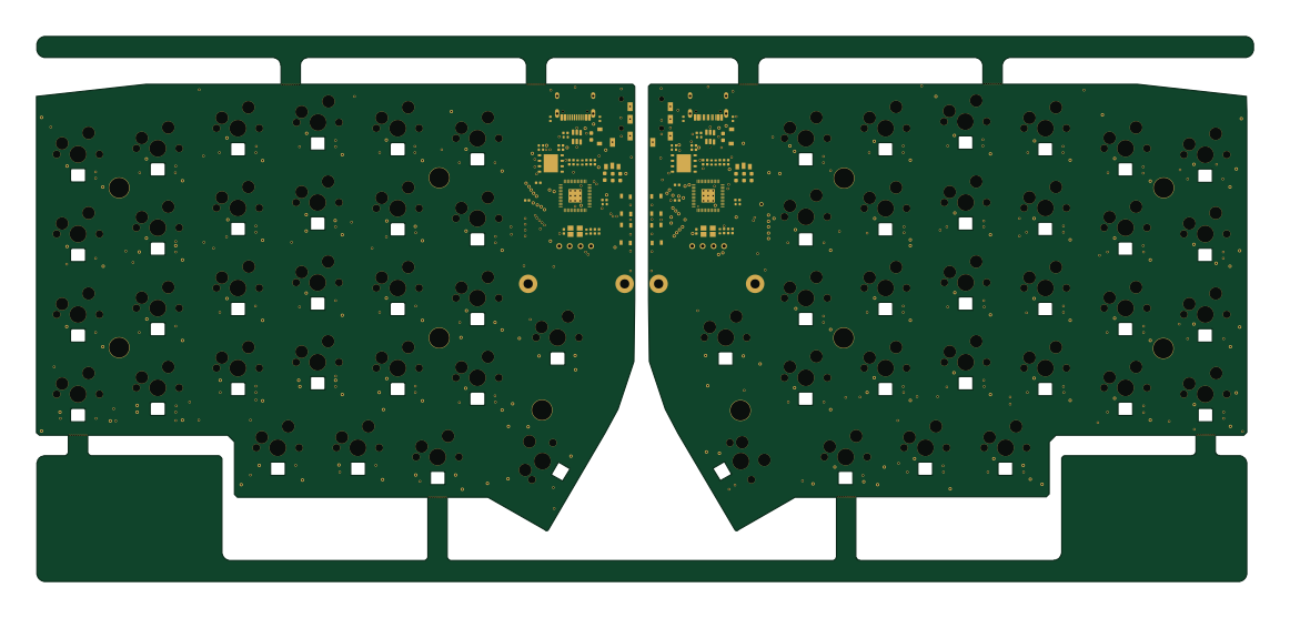 RP2040/RP2350
Pro V2
kata0510
290.1 × 130 mm270 parts2LMIT2.3k