
Low noise power probe

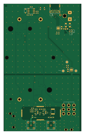
About the Low noise power probe PCB
Low noise power probe is an open source PCB design by blinken, published on GitHub under the CC-BY-SA-4.0 license. It is a 6-layer board measuring 69.7 × 114.8 mm, with 105 components from 43 distinct parts.
Other key parts include the OPA354, ADP7142AUJZ-2.5, MCP73213T-A6SI/MF, ADP7182AUJZ-2.5 and HUSB238. By type, the board carries 35 resistors, 20 capacitors, 15 diodes, 12 ICs, 8 connectors and 7 transistors.
It belongs with the test & measurement and power & battery designs in this gallery.
From the project
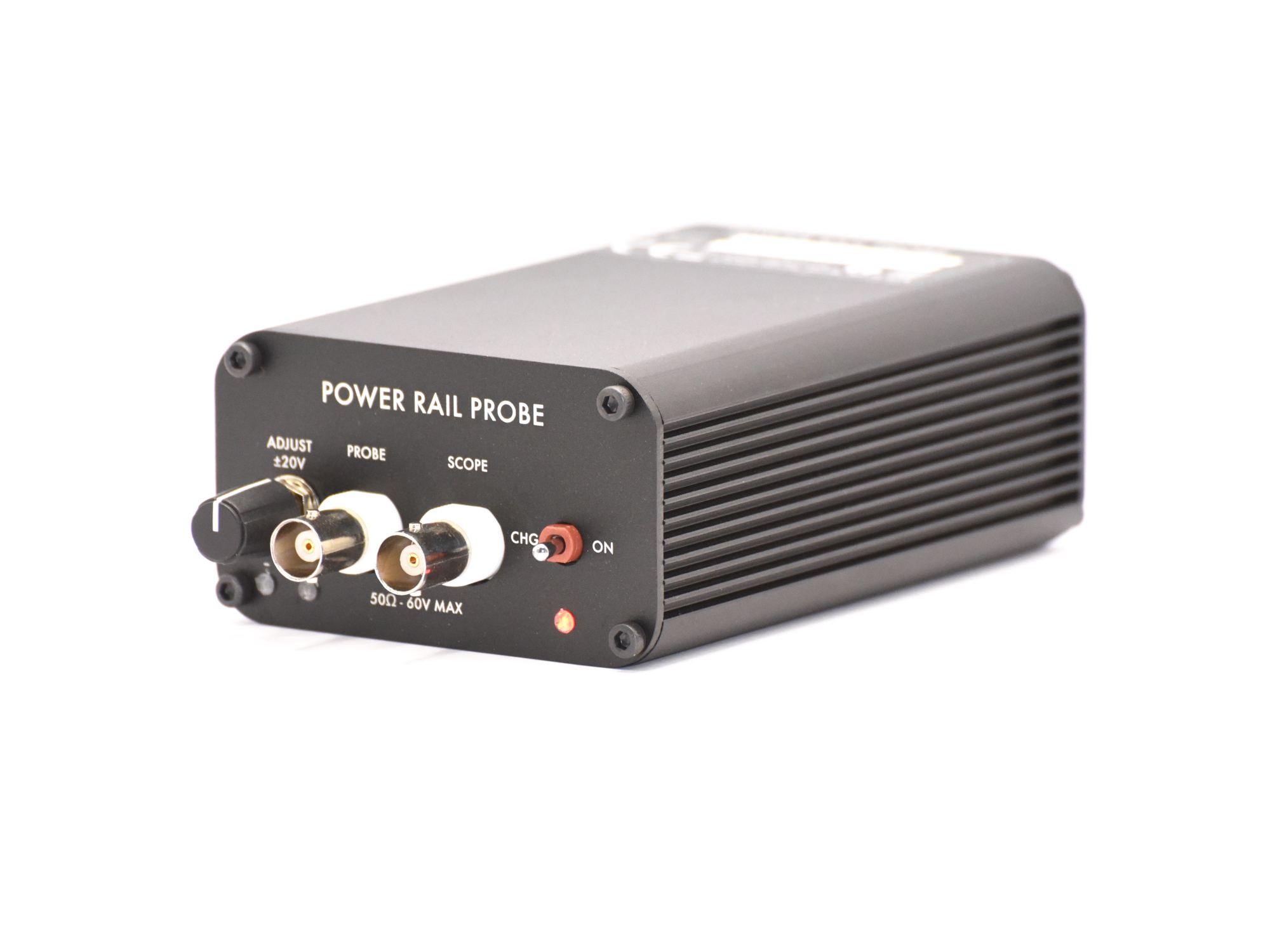
Low-noise oscilloscope power rail probe
An Open Hardware low-noise power rail oscilloscope probe, loosely based on the excellent writeup by Andrew Levido [PDF archive].
The probe allows you to measure millivolt-level ripple on a power rail up to 20V, using a normal oscilloscope, by applying a vertical offset. This open design costs <10% of the price of the Tektronix TPR1000.
Measurement of 60mV p-p ripple on a 20V rail (ie. ripple 19.97V - 20.03V) using an inexpensive Picoscope 2204A
Main components on the Low noise power probe
Low noise power probe bill of materials (BOM)
105 components, 43 distinct parts — part numbers from the project's BOM.
| Qty | Part | Footprint | Refs |
|---|---|---|---|
| 2 | OPA354 | SOT-23-5 | U1, U2 |
| 1 | ADP7142AUJZ-2.5 | TSOT-23-5 | U3 |
| 1 | MCP73213T-A6SI/MF | DFN-10-1EP_3x3mm_P0.5mm_EP1.55x2.48mm | U4 |
| 1 | ADP7182AUJZ-2.5 | TSOT-23-5 | U5 |
| 1 | HUSB238 | DFN-10-1EP_3x3mm_P0.5mm_EP1.65x2.38mm | U6 |
| 1 | LM334DT | SO-8_3.9x4.9mm_P1.27mm | U7 |
| 1 | LM311DR | SOIC-8_3.9x4.9mm_P1.27mm | U8 |
| 2 | HY2213 | SOT-23-6 | U10, U13 |
| 2 | DW01A | SOT-23-6 | U11, U12 |
| 1 | WSE3099 | SOT-89-3 | Q1 |
| 6 | HL2312 | SOT-23 | Q2, Q3, Q4, Q5, Q6, Q7 |
| 2 | Amphenol 901-10138 | SMA_Amphenol_901-10138_Horizontal | J1, J2 |
| 1 | DC-005 2.0 | BarrelJack_Horizontal | J3 |
| 1 | USB_C_Receptacle | USB_C_Receptacle_Molex_105450-0101 | J4 |
| 4 | RF Shield Clip | ICSRC6508-015SFR | J8, J9, J11, J12 |
| 1 | Dual_Battery_Cell | Battery-holder-18650-MYOUNG-BH-18650-A1BJ021 | BT1 |
| 4 | SMD1206-050C-24V | Fuse_1206_3216Metric | F1, F2, F3, F4 |
| 1 | 5k | Potentiometer_Nidec_M-1303 | RV1 |
| 1 | SW_3PDT_x3 | Switch_3PDT_C&K_7301MD9ABE | SW1 |
| 5 | Red 1.8V | LED_0603_1608Metric_polaritysilk | D1, D3, D4, D5, D6 |
Show 23 more
| Qty | Part | Footprint | Refs |
|---|---|---|---|
| 1 | 3V3 | D_SOD-123 | D2 |
| 2 | 1N5819WS | D_SOD-323 | D7, D8 |
| 7 | SD24-MS | D_SOD-323_silkpolarity | D9, D10, D11, D12, D13, D14, D15 |
| 1 | 10uH 5% | L_1812_4532Metric | L1 |
| 1 | 100n / SRF 28MHz | C_0402_1005Metric | C1 |
| 17 | 2.2u | C_0402_1005Metric | C2, C3, C4, C5, C6, C7, C8, C10 +9 |
| 2 | 10uF | C_0805_2012Metric | C9, C14 |
| 1 | 2R2 1% 400ppm/°C | R_0603_1608Metric | R1 |
| 2 | 50k .1% | R_0603_1608Metric | R2, R3 |
| 1 | 1.21k 1% 100ppm/°C | R_0603_1608Metric | R4 |
| 1 | 3.3k | R_0603_1608Metric | R5 |
| 1 | 1k .1% | R_0603_1608Metric | R6 |
| 1 | 10R 1% 200ppm/°C | R_0603_1608Metric | R7 |
| 5 | 1k | R_0603_1608Metric | R8, R21, R23, R33, R35 |
| 2 | 5k | R_0603_1608Metric | R9, R38 |
| 3 | 50k | R_0603_1608Metric | R10, R22, R24 |
| 6 | 10R 200mW | R_0603_1608Metric | R11, R27, R28, R29, R30, R32 |
| 2 | 6.04k | R_0603_1608Metric | R12, R14 |
| 2 | 0R | R_0603_1608Metric | R13, R26 |
| 1 | 10M | R_0603_1608Metric | R15 |
| 2 | 620 | R_0603_1608Metric | R16, R17 |
| 1 | 33R | R_0603_1608Metric | R20 |
| 4 | 100R | R_0603_1608Metric | R31, R36, R37, R39 |
Low noise power probe design files
The KiCad project lives in the blinken/power-rail-probe repository on GitHub; these links point at the commit this page was built from.
Low noise power probe: common questions
How big is the Low noise power probe PCB?
The Low noise power probe measures 69.7 × 114.8 mm, has 6 copper layers and is 4.69 mm thick.
How many components are on the Low noise power probe?
105 components, from 43 distinct parts, with part numbers taken from the project's own BOM. The full bill of materials is listed on this page.
Where can I download the Low noise power probe design files?
From the blinken/power-rail-probe repository on GitHub, which has the KiCad layout, the schematic and the BOM; the links under Design files point to each one.
Can I use the Low noise power probe design in my own project?
Yes, under the terms of its CC-BY-SA-4.0 license, which blinken chose for the repository.
More boards in power-rail-probe
Similar boards

Display Carrier
AxxAxx
35.6 × 58.2 mm5 parts2LGPL-3.01.7k
ControllerCurrentShuntAddOn
stuartpittaway
26 × 16.9 mm9 parts2LCC-BY-NC-4.01.1k
TemperaturePCB PANEL
116 × 75.5 mm178 parts2LCC-BY-NC-4.01.1k
Module 16S PassiveBalanceAddOn
61 × 74 mm86 parts2LCC-BY-NC-4.01.1k
ProgrammingAdapter
10.5 × 83 mm3 parts2LCC-BY-NC-4.01.1k
Cube batteryboard
willem-pennings
95 × 95 mm4 parts2LGPL-3.01.1k