
Debug Adapter

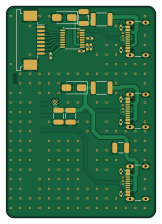
About the Debug Adapter PCB
Debug Adapter is an open source PCB design by Bogdan8266, published on GitHub under the CERN-OHL-P-2.0 license. It is a 2-layer board measuring 39.5 × 56 mm, with 25 components from 10 distinct parts.
Other key parts include the Genesys Logic. By type, the board carries 9 capacitors, 6 resistors, 5 connectors, 2 fuses, 2 diodes and 1 IC.
It belongs with the power & battery, iot & wireless and dev boards & breakouts designs in this gallery.
From the project
8-layer Allwinner H616/618 SBC with DDR3, USB, Wi-Fi/BT and battery power support, designed for embedded Linux.
A compact, battery-powered 64-bit ARM development board measuring 50 mm × 50 mm based on the Allwinner H616 Quad-Core Cortex-A53 SoC with integrated powerbank PMU, high-speed DDR3, eMMC 5.1, and dual-band Wi-Fi.
Unlike standard commercial H616 boards (Orange Pi, Banana Pi, etc.) that require a 5V/3A wall adapter and shut down the moment you unplug the cable, Nebula Board features an onboard bidirectional fast-charging system that runs from a single Li-ion cell (18650 / Li-Po) and recharges via USB-C with USB-PD / QC4+.
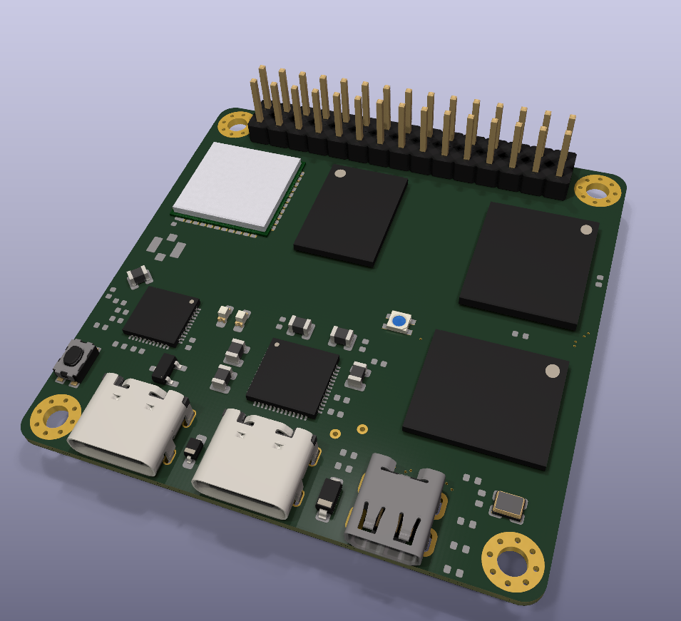
Main components on the Debug Adapter
Debug Adapter bill of materials (BOM)
25 components, 10 distinct parts.
| Qty | Part | Footprint | Refs |
|---|---|---|---|
| 1 | Genesys Logic GL823K GL823K-HCY04 | SSOP-16_3.9x4.9mm_P0.635mm | U1 |
| 3 | TYPE-C-31-M-12 USB_C_Receptacle_USB2.0_16P Korean Hroparts Elec | USB_C_Receptacle_GCT_USB4105-xx-A_16P_TopMnt_Horizontal | J2, J6, J7 |
| 1 | XW10202-08R-00 Conn_01x08_MountingPin HCTL | TE_84952-8_1x08-1MP_P1.0mm_Horizontal | J3 |
| 1 | XW10202-20R-00 Conn_01x20_MountingPin HCTL | TE_2-84952-0_1x20-1MP_P1.0mm_Horizontal | J5 |
| 2 | SMD1812-200C-30V Fuse_Small BNstar | Fuse_1812_4532Metric_Pad1.30x3.40mm_HandSolder | F1, F2 |
| 2 | SMAJ5.0A FUXINSEMI | D_SMA | D1, D2 |
| 5 | GRM155R61A106ME44D 10u Murata Electronics | C_0402_1005Metric_Pad0.74x0.62mm_HandSolder | C1, C2, C3, C4, C5 |
| 4 | CS3225X7R476K160NRL 47u Samwha Capacitor | C_1210_3225Metric_Pad1.33x2.70mm_HandSolder | C7, C8, C9, C10 |
| 4 | RC0402FR-075K1L 5K1 YAGEO | R_0402_1005Metric | R2, R3, R4, R5 |
| 2 | RC0402FR-0722KL 22K YAGEO | R_0402_1005Metric | R6, R7 |
Debug Adapter design files
The KiCad project lives in the Bogdan8266/h616-board repository on GitHub; these links point at the commit this page was built from.
Debug Adapter: common questions
How big is the Debug Adapter PCB?
The Debug Adapter measures 39.5 × 56 mm, has 2 copper layers and is 1.6 mm thick.
How many components are on the Debug Adapter?
25 components, from 10 distinct parts. The full bill of materials is listed on this page.
Where can I download the Debug Adapter design files?
From the Bogdan8266/h616-board repository on GitHub, which has the KiCad layout and the schematic; the links under Design files point to each one.
Can I use the Debug Adapter design in my own project?
Yes, under the terms of its CERN-OHL-P-2.0 license, which Bogdan8266 chose for the repository.
More boards in h616-board
Similar boards
EinkPDA screen
TalismanDesign
95 × 54 mm27 parts2LApache-2.02.0k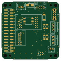
Stack chan
stack-chan
50 × 50 mm33 parts2LApache-2.01.7k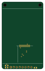
Display Carrier
AxxAxx
35.6 × 58.2 mm5 parts2LGPL-3.01.7k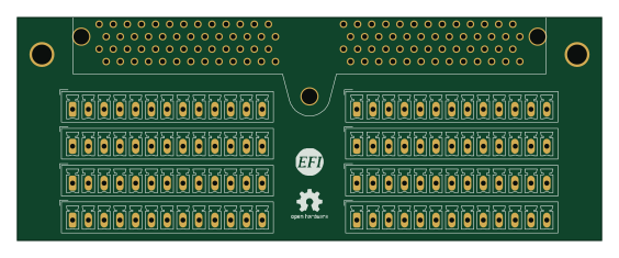
Eecv breakout
rusefi
140.8 × 53.7 mm9 parts4LGPL-3.01.2k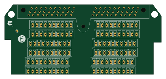
Breakout 60pin EEC-IV
139.7 × 62.2 mm15 parts2LGPL-3.01.2k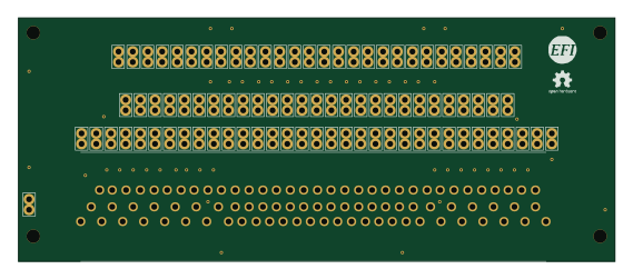
88 Pin Vag Breakout
142 × 58 mm91 parts2LGPL-3.01.2k