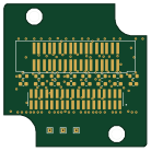
Source splitter

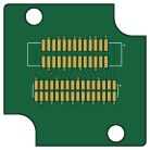
About the Source splitter PCB
Source splitter is an open source PCB design by BUNPC, published on GitHub. It is a 2-layer board measuring 34.5 × 34.5 mm, with 3 components from 3 distinct parts.
From the project
Repository for the storage and dissemination of NN22 technical documents
All source related files are located within this folder.
Two versions of the backplane are available, the 7 layer and single layer. - The 7 layer folder contains the files for the full height backplane to allow for up to 7 source interface cards to be connected. - The single layer folder contains the files for the system configuration with only one interface card per backboard slot.
Source splitter bill of materials (BOM)
3 components, 3 distinct parts — part numbers from the project's BOM.
| Qty | Part | Footprint | Refs |
|---|---|---|---|
| 1 | Conn_02x13_Odd_Even | SAMTEC_SHF-113-01-L-D-SM | J1 |
| 1 | Conn_02x16_Odd_Even | SAMTEC_SFMC-116-02-S-D_swap12 | J2 |
| 1 | Housing | 1551QGY | N1 |
Source splitter design files
The KiCad project lives in the BUNPC/NN22-Technical-Documents repository on GitHub; these links point at the commit this page was built from.
- LayoutHardware Main/Electronics/Source Electronics/SRC_Splitter/source-splitter.kicad_pcb
- SchematicHardware Main/Electronics/Source Electronics/SRC_Splitter/source-splitter.kicad_sch
- BOMHardware Peripherial/ninjaNIRS Triggerbox/hardware/Rev1a_Eagle/T-Y16W206116A W206116ASY15-10sets-TriggerBox_Rev1a_BOM-Elsa2020.11.23.xlsx
Source splitter: common questions
How big is the Source splitter PCB?
The Source splitter measures 34.5 × 34.5 mm, has 2 copper layers and is 1.6 mm thick.
How many components are on the Source splitter?
3 components, from 3 distinct parts, with part numbers taken from the project's own BOM. The full bill of materials is listed on this page.
Where can I download the Source splitter design files?
From the BUNPC/NN22-Technical-Documents repository on GitHub, which has the KiCad layout, the schematic and the BOM; the links under Design files point to each one.
Can I use the Source splitter design in my own project?
The repository has no license, so all rights stay with BUNPC. Use it as a reference, and ask the author before reusing the design.