
Fancy node

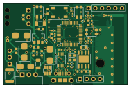
About the Fancy node PCB
Fancy node is an open source STM32 PCB design by candykingdom, published on GitHub. It is a 4-layer board measuring 47.1 × 30.7 mm, with 66 components from 36 distinct parts.
Its main chip is the STM32G070CBTX, from the STM32 family. Other key parts include the CH340X, WS2812B, HT75XX-1-SOT89, RFM69CW-915MHZ and TP4056. By type, the board carries 19 resistors, 18 capacitors, 8 diodes, 7 connectors, 6 ICs and 4 switches.
It belongs with the rf & radio designs in this gallery.
From the project
Small blinkenlight boards that sync up using radios
Wireless LED control for Burning Man art installations, bikes, and wearables. Devices driving WS2812 strips self-organize over 915 MHz RFM69 radios into a flood mesh with exactly one master, share a network clock via heartbeats, and render effects as pure functions of network time — so every device animates in sync without streaming frames.
New to the project? Start with GETTING_STARTED.md. Working in the code (human or agent)? The mental model lives in docs/index.md and the shared Claude Code/Codex ground rules in CLAUDE.md.
Main components on the Fancy node
Fancy node bill of materials (BOM)
66 components, 36 distinct parts — part numbers from the project's BOM.
| Qty | Part | Footprint | Refs |
|---|---|---|---|
| 1 | CH340X | MSOP-10_3x3mm_P0.5mm | U1 |
| 1 | WS2812B WS2812b | LED_XINGLIGHT_WS2812B_PLCC4_5.0x5.0mm_P3.2mm | U3 |
| 1 | HT75XX-1-SOT89 HT75xx-1-SOT89 | SOT-89-3 | U4 |
| 1 | RFM69CW-915MHZ | RFM69CW-minimalpads | U5 |
| 1 | TP4056 | SOP-8_3.9x4.9mm_P1.27mm_Thermal | U6 |
| 1 | STM32G070CBTX STM32G070CBTx | LQFP-48_7x7mm_P0.5mm | U7 |
| 1 | C132563 USB_B_Micro | FRAMATOME_10118194-0001LF_fixed_bridges | J1 |
| 1 | Conn_01x06 | PinHeader_1x06_P2.54mm_Vertical | J2 |
| 1 | Conn_01x03 | PinHeader_1x03_P2.54mm_Horizontal | J3 |
| 1 | Conn_01x03 | MiniPV_78208-X03XXX_1x03_P2.54mm_Polarized_Horizontal | J4 |
| 1 | Conn_01x04 | PinHeader_1x04_P2.54mm_Vertical | J5 |
| 1 | Conn_01x02 | JST_Micro_1x02_P1.25mm_Horizontal | J6 |
| 1 | 2337019-1 | CONN_2337019-1 | J7 |
| 1 | StrainRelief | 3_pin_2.54mm_pitch_strain_relief | H1 |
| 1 | SolderJumper_2_Open | SolderJumper-2_P1.3mm_Open_TrianglePad1.0x1.5mm | JP2 |
| 3 | SW_Push | SW_TACTILE_3mmx3.5mm_TS-1071SA-A4B3-D4 | SW1, SW2, SW3 |
| 1 | C2909229 SW_SPDT | SW_SLIDE_SPDT_K3-1204D-L | SW4 |
| 1 | C89650 Thermistor_PTC | Fuse_1812_4532Metric_Pad1.30x3.40mm_HandSolder | TH1 |
| 2 | C2286 RED | LED_0603_1608Metric | D1, D7 |
| 1 | SRV05-4-P-T7 | SOT-23-6 | D2 |
Show 16 more
| Qty | Part | Footprint | Refs |
|---|---|---|---|
| 3 | C78395 D_TVS | D_SMB | D3, D4, D5 |
| 1 | C2290 WHITE | LED_0603_1608Metric | D6 |
| 1 | C8678 D | D_SMA | D8 |
| 1 | 33NH 27nH | L_0402_1005Metric | L1 |
| 8 | 100NF 100nF | C_0402_1005Metric_Pad0.74x0.62mm_HandSolder | C1, C2, C3, C5, C7, C9, C13, C15 |
| 7 | 10UF 10uF | C_0603_1608Metric | C4, C6, C8, C11, C12, C16, C18 |
| 2 | 47UF 47uF | C_1206_3216Metric | C10, C14 |
| 1 | 1pF | C_0402_1005Metric_Pad0.74x0.62mm_HandSolder | C17 |
| 11 | 1k | R_0402_1005Metric | R1, R2, R3, R4, R5, R6, R7, R12 +3 |
| 1 | 4K7 4k7 | R_0402_1005Metric | R8 |
| 1 | 470 | R_0603_1608Metric | R9 |
| 1 | 62K 62k | R_0603_1608Metric | R10 |
| 1 | 180K 180k | R_0603_1608Metric | R11 |
| 1 | 3K3 3k3 | R_0603_1608Metric | R14 |
| 2 | 220 | R_0402_1005Metric | R16, R19 |
| 1 | 10K 10k | R_0402_1005Metric | R18 |
Fancy node design files
The KiCad project lives in the candykingdom/firefly2 repository on GitHub; these links point at the commit this page was built from.
Fancy node: common questions
What microcontroller does the Fancy node use?
The Fancy node is built around the STM32G070CBTX, from the STM32 family.
How big is the Fancy node PCB?
The Fancy node measures 47.1 × 30.7 mm, has 4 copper layers and is 1.6 mm thick.
How many components are on the Fancy node?
66 components, from 36 distinct parts, with part numbers taken from the project's own BOM. The full bill of materials is listed on this page.
Where can I download the Fancy node design files?
From the candykingdom/firefly2 repository on GitHub, which has the KiCad layout, the schematic and the BOM; the links under Design files point to each one.
Can I use the Fancy node design in my own project?
The repository has no license, so all rights stay with candykingdom. Use it as a reference, and ask the author before reusing the design.
Can I test firmware for the Fancy node without the hardware?
Yes. HardLabs builds a simulation of the board from its netlist and BOM, so you can run and debug STM32 firmware against it before you order a PCB.
More boards in firefly2
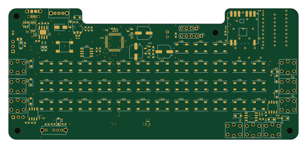 STM32
Controller
150 × 68 mm190 parts2LNo license5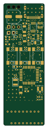 STM32
Rfboard
21 × 63 mm67 parts4LNo license5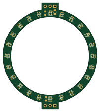
Ring-50mm
50.2 × 56.6 mm53 parts2LNo license5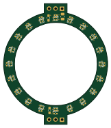
Ring-40mm
40.1 × 46.4 mm45 parts2LNo license5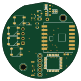 STM32
Firefly2
41.4 × 41.3 mm21 parts2LNo license5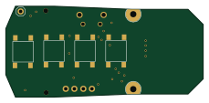 STM32
Rf remote
57.3 × 26.5 mm12 parts2LNo license5
Similar boards
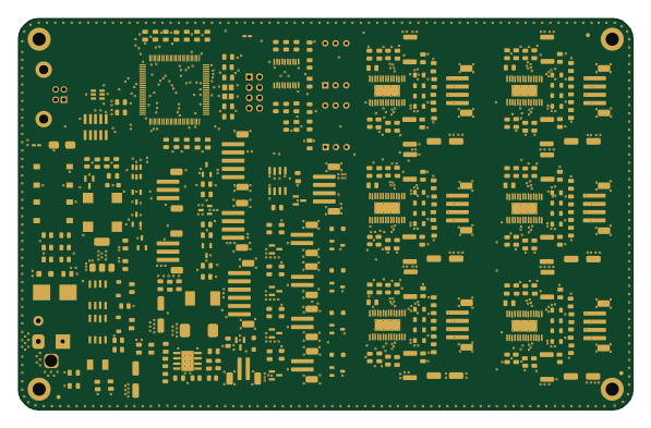 STM32
LumenPnP Motherboard
opulo-inc
149 × 95 mm296 parts4LCC-BY-SA-4.03.7k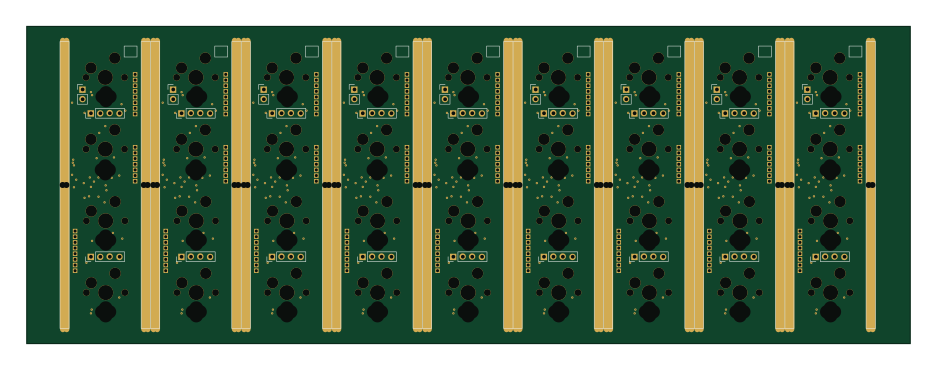 STM32
Main panel
google
234 × 84 mm26 parts4LApache-2.02.9k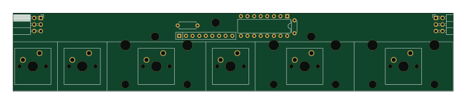 STM32
Type g
169 × 30 mm24 parts2LApache-2.02.9k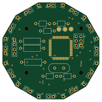 STM32
Base
52.3 × 52.3 mm36 parts2LApache-2.02.9k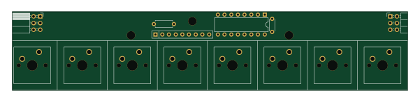 STM32
Type a
150 × 30 mm14 parts2LApache-2.02.9k STM32
Type c
188 × 30 mm17 parts2LApache-2.02.9k