
Pcb ch552 devboard

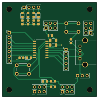
About the Pcb ch552 devboard
Pcb ch552 devboard is an open source WCH CH32/CH55x PCB design by cfrankb, published on GitHub. It is a 2-layer board measuring 50 × 50 mm, with 29 components from 13 distinct parts.
Its main chip is the CH552G, from the WCH CH32/CH55x family. By type, the board carries 9 connectors, 8 resistors, 6 diodes, 3 capacitors, 2 switches and 1 IC.
It belongs with the dev boards & breakouts and test & measurement designs in this gallery.
From the project
CH552 Devboard with ON/OFF switch, BOOT and RESET buttons. Indicator lights and lots of pins.
This is a pcb design for a CH552 DEVBOARD. The board is intended to aid in the development of firmware/prototype for the CH552 and CH554 microcontrollers.
* The Power Switch (Workflow Optimization): The CH552 enters ISP (programming) mode based on power-on state with a specific pin held. Constantly pulling a USB cable wears out the connector and is inefficient. Your switch demonstrates mechanical sympathy and an understanding of the iterative development cycle.
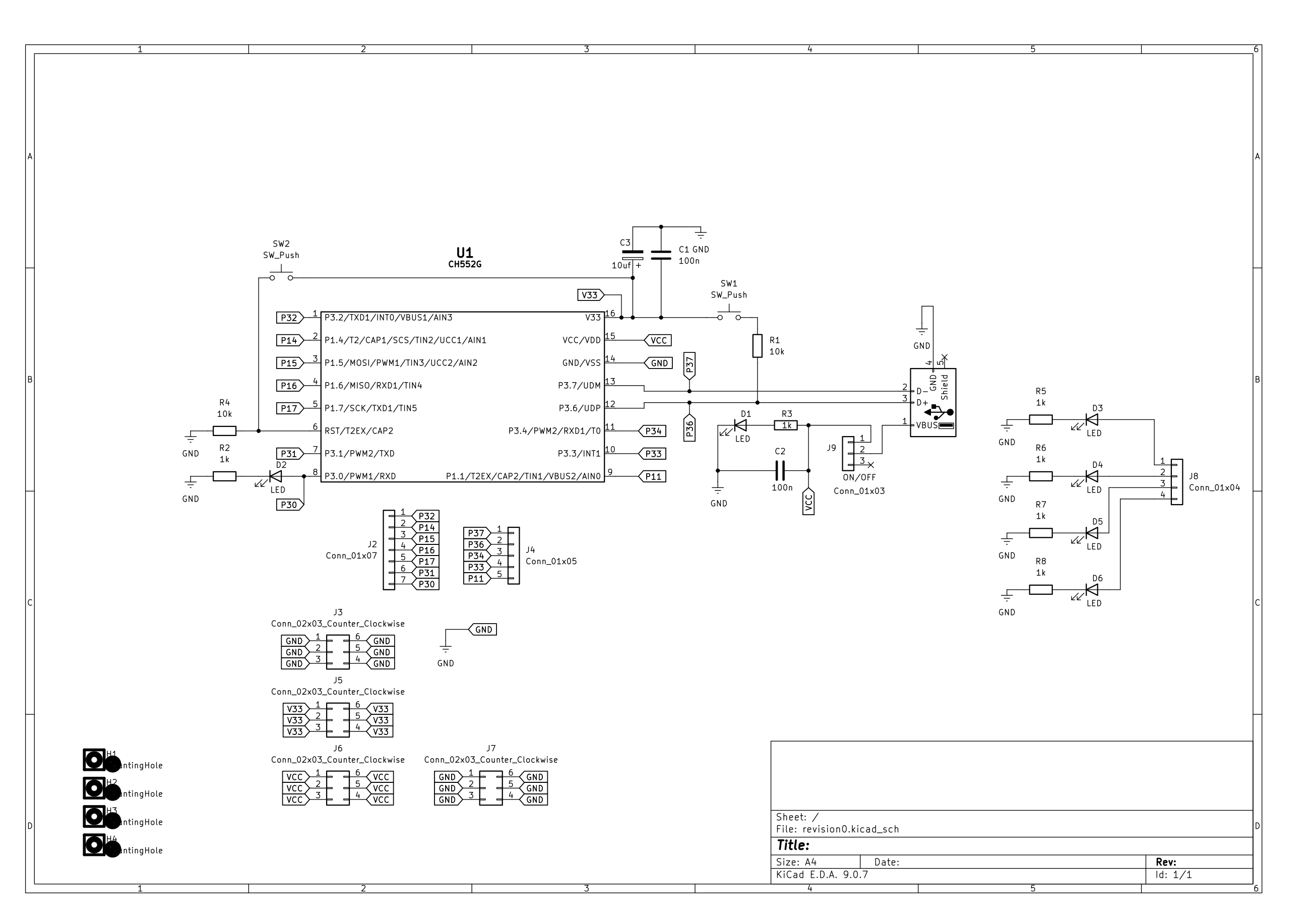
Main components on the Pcb ch552 devboard
Pcb ch552 devboard bill of materials (BOM)
29 components, 13 distinct parts.
| Qty | Part | Footprint | Refs |
|---|---|---|---|
| 1 | CH552G | SOP-16_4.55x10.3mm_P1.27mm | U1 |
| 1 | USB1 | USB_A_Molex_67643_Horizontal | J1 |
| 1 | Conn_01x07 | PinHeader_1x07_P2.54mm_Vertical | J2 |
| 4 | Conn_02x03_Counter_Clockwise | PinHeader_2x03_P2.54mm_Vertical | J3, J5, J6, J7 |
| 1 | Conn_01x05 | PinHeader_1x05_P2.54mm_Vertical | J4 |
| 1 | Conn_01x04 | PinHeader_1x04_P2.54mm_Vertical | J8 |
| 1 | Conn_01x03 | PinHeader_1x03_P2.54mm_Vertical | J9 |
| 2 | SW_Push | SW_PUSH_6mm_H4.3mm | SW1, SW2 |
| 6 | LED | LED_0805_2012Metric_Pad1.15x1.40mm_HandSolder | D1, D2, D3, D4, D5, D6 |
| 2 | 100n | C_1206_3216Metric_Pad1.33x1.80mm_HandSolder | C1, C2 |
| 1 | 10uf | C_0805_2012Metric_Pad1.18x1.45mm_HandSolder | C3 |
| 2 | 10k | R_0805_2012Metric_Pad1.20x1.40mm_HandSolder | R1, R4 |
| 6 | 1k | R_0805_2012Metric_Pad1.20x1.40mm_HandSolder | R2, R3, R5, R6, R7, R8 |
Pcb ch552 devboard design files
The KiCad project lives in the cfrankb/pcb_ch552_devboard repository on GitHub; these links point at the commit this page was built from.
- Layoutrevision0/revision0.kicad_pcb
- Schematicrevision0/revision0.kicad_sch
Pcb ch552 devboard: common questions
What microcontroller does the Pcb ch552 devboard use?
The Pcb ch552 devboard is built around the CH552G, from the WCH CH32/CH55x family.
How big is the Pcb ch552 devboard?
The Pcb ch552 devboard measures 50 × 50 mm, has 2 copper layers and is 1.6 mm thick.
How many components are on the Pcb ch552 devboard?
29 components, from 13 distinct parts. The full bill of materials is listed on this page.
Where can I download the Pcb ch552 devboard design files?
From the cfrankb/pcb_ch552_devboard repository on GitHub, which has the KiCad layout and the schematic; the links under Design files point to each one.
Can I use the Pcb ch552 devboard design in my own project?
The repository has no license, so all rights stay with cfrankb. Use it as a reference, and ask the author before reusing the design.
Can I test firmware for the Pcb ch552 devboard without the hardware?
Yes. HardLabs builds a simulation of the board from its netlist and BOM, so you can run and debug WCH CH32/CH55x firmware against it before you order a PCB.
Similar boards
 WCH CH32/CH55x
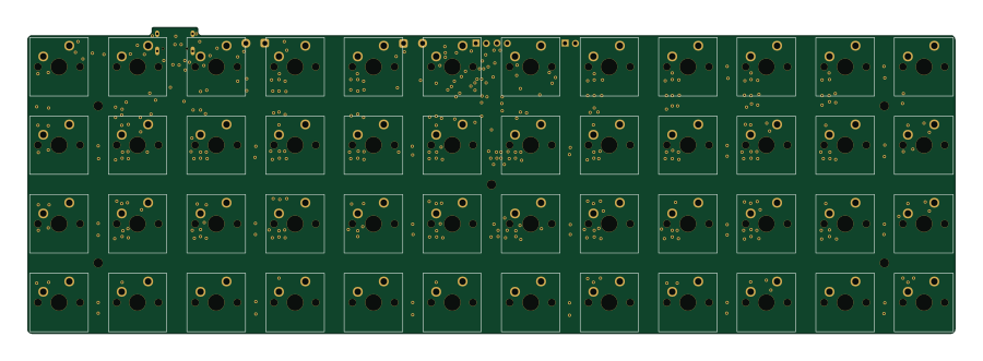
CH32X-48
rgoulter
224.6 × 74.2 mm112 parts2LNo license230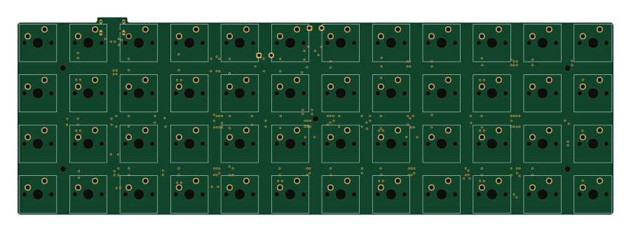 WCH CH32/CH55x
CH552-48
224.6 × 74.2 mm107 parts2LNo license230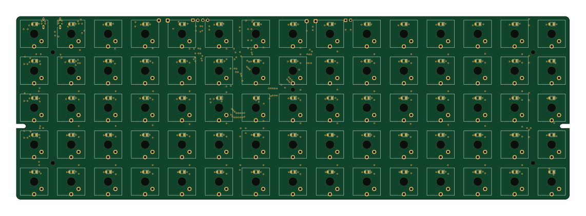 WCH CH32/CH55x
CH32X-75
285 × 94.2 mm318 parts2LNo license230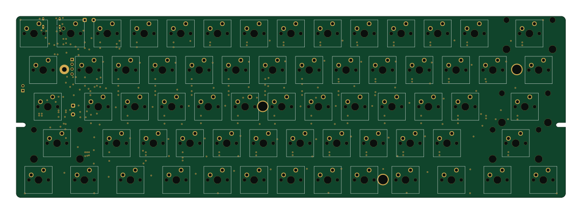 WCH CH32/CH55x
CH32X-60-ANSI-Improved
285 × 94.2 mm149 parts2LNo license230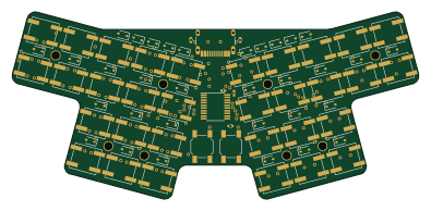 WCH CH32/CH55x
Idawgz32
ChrisChrisLoLo
98.7 × 45.5 mm81 parts2LGPL-3.077 WCH CH32/CH55x
Pointify
luftaquila
23.1 × 20.7 mm8 parts2LGPL-3.042