
Routed base

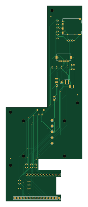
About the Routed base PCB
Routed base is an open source PCB design by dpaola2, published on GitHub. It is a 4-layer board measuring 66 × 169 mm, with 36 components from 15 distinct parts.
Other key parts include the TPS62162DSGR. By type, the board carries 21 resistors, 7 capacitors, 5 connectors, 1 IC, 1 fuse and 1 inductor.
It belongs with the rf & radio, iot & wireless and displays & leds designs in this gallery.
From the project
Current logistics, September 26: core modules are received, and the revision B shells, LCD supports and carrier gauge passed loose fit checks. Screws and foam are ordered. The SD trial playlist is prepared. The assembled carrier remains unordered. A supplier quote request was sen
Current logistics, September 26: core modules are received, and the revision B shells, LCD supports and carrier gauge passed loose fit checks. Screws and foam are ordered. The SD trial playlist is prepared. The assembled carrier remains unordered. A supplier quote request was sent to PCBWay for DFM review and pricing; the response is pending. Physical mating, cable mapping and powered qualification remain open. The historical design record below retains its original dated assumptions.
Main components on the Routed base
Routed base bill of materials (BOM)
36 components, 15 distinct parts — part numbers from the project's BOM.
| Qty | Part | Footprint | Refs |
|---|---|---|---|
| 1 | TPS62162DSGR TPS62162DSGR / 3.3V | WSON-8-1EP_2x2mm_P0.5mm_EP0.9x1.6mm_ThermalVias | U1 |
| 1 | SSW-116-01-G-S Feather JP1 socket | PinSocket_1x16_P2.54mm_Vertical | J1 |
| 1 | SSW-112-01-G-S Feather JP3 socket | PinSocket_1x12_P2.54mm_Vertical | J2 |
| 1 | EYESPI ribbon | Hirose_FH12-18S-0.5SH_1x18-1MP_P0.50mm_Horizontal | J3 |
| 1 | DM3AT-SF-PEJM5 Dedicated microSD | microSD_HC_Hirose_DM3AT-SF-PEJM5 | J4 |
| 1 | ANO #6310 cable | JST_SH_SM04B-SRSS-TB_1x04-1MP_P1.00mm_Horizontal | J5 |
| 1 | MF-NSMF075-2 0.75A hold PTC | Fuse_1206_3216Metric | F1 |
| 1 | XFL4020-222MEC 2.2uH | L_Coilcraft_XxL4020 | L1 |
| 2 | C3225X7R1C226M250AC 22uF | C_1210_3225Metric | C1, C2 |
| 3 | C0805C104K5RACTU 100nF | C_0805_2012Metric | C3, C5, C7 |
| 2 | C2012X7R1A106K125AC 10uF | C_0805_2012Metric | C4, C6 |
| 10 | RC0603FR-07100RL 100R | R_0603_1608Metric | R1, R2, R3, R4, R5, R6, R7, R8 +2 |
| 6 | RC0603FR-0747KL 47k | R_0603_1608Metric | R11, R12, R13, R14, R15, R16 |
| 3 | RC0603FR-0710KL 10k | R_0603_1608Metric | R17, R18, R19 |
| 2 | RC0603FR-07100KL 100k | R_0603_1608Metric | R20, R21 |
Routed base design files
The KiCad project lives in the dpaola2/Harmony repository on GitHub; these links point at the commit this page was built from.
Routed base: common questions
How big is the Routed base PCB?
The Routed base measures 66 × 169 mm, has 4 copper layers and is 1.6 mm thick.
How many components are on the Routed base?
36 components, from 15 distinct parts, with part numbers taken from the project's own BOM. The full bill of materials is listed on this page.
Where can I download the Routed base design files?
From the dpaola2/Harmony repository on GitHub, which has the KiCad layout and the BOM; the links under Design files point to each one.
Can I use the Routed base design in my own project?
The repository has no license, so all rights stay with dpaola2. Use it as a reference, and ask the author before reusing the design.
More boards in Harmony
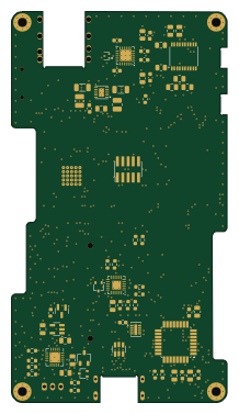 ESP32
ESP32Tangara mainboard
52 × 94.2 mm95 parts4LNo license0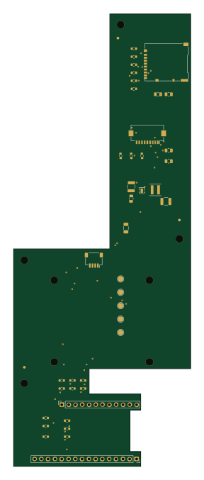
Harmony mark6-carrier
66.2 × 169 mm36 parts4LNo license0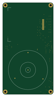
Tangara faceplate
52 × 94.2 mm22 parts2LNo license0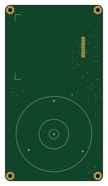
Faceplate refilled native
52 × 94.2 mm22 parts2LNo license0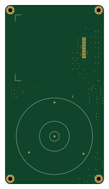
Faceplate net aware before refill
52 × 94.2 mm22 parts2LNo license0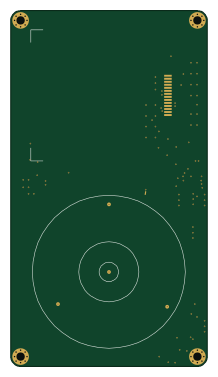
Faceplate before
52 × 94.2 mm22 parts2LNo license0
Similar boards
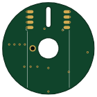
View screen
scottbez1
35 × 35 mm12 parts2LApache-2.022.2k
BM28B0.6-24DSBreakout
15.2 × 35.6 mm3 parts2LApache-2.022.2k
LevelShifterBreakout
15.2 × 20.3 mm5 parts2LApache-2.022.2k
View base
81.2 × 81.2 mm81 parts2LApache-2.022.2k
ChainlinkDriverTester
198.1 × 95.3 mm123 parts2LApache-2.04.2k
ChainlinkBase
98.4 × 190.5 mm119 parts2LApache-2.04.2k