
Breakout

About the Breakout
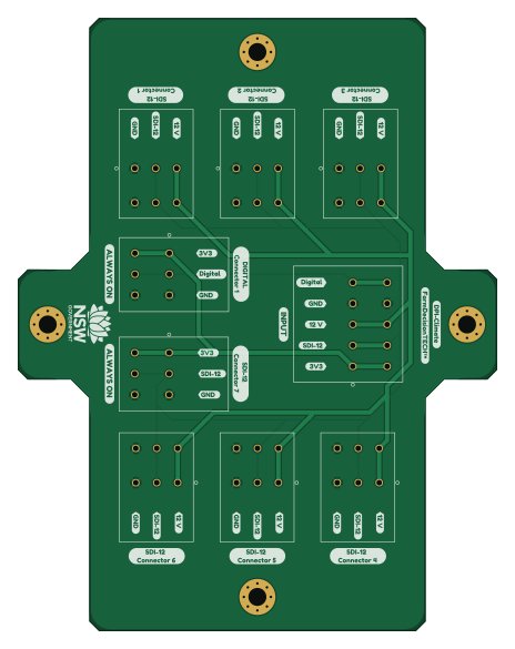
Breakout is an open source PCB design by DPIclimate, published on GitHub under the MIT license. It is a 2-layer board measuring 114.1 × 146.1 mm, with 9 components from 2 distinct parts.
It belongs with the iot & wireless, power & battery and sensors designs in this gallery.
From the project
Agriculture node for SDI-12 (and other) sensors.
Enviro-node is a environmental monitoring node. Users can connect a number of sensors to a node. Data captured from these sensors is then sent to a database over MQTT.
The hardware was developed using KiCad. Source files can be found here. While sleeping the Enviro-node will consume ~70 µA.
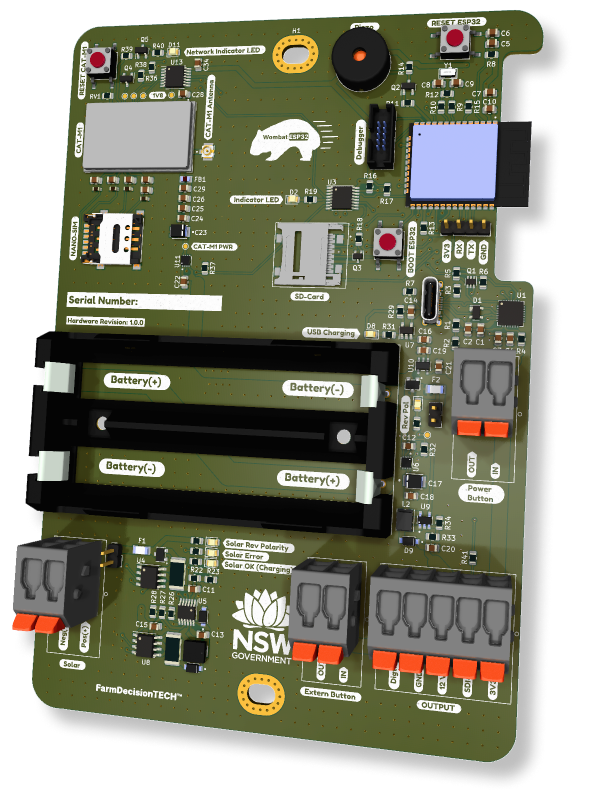
The device incorporates a ESP32 microcontroller to handle bluetooth functions and peripherals. The ESP32 has a very low sleep current of ~16 µA making it perfect for low-powered applications.
Breakout bill of materials (BOM)
9 components, 2 distinct parts.
| Qty | Part | Footprint | Refs |
|---|---|---|---|
| 8 | 2604-3103 | 2604-3103 | J1, J2, J3, J4, J5, J6, J7, J9 |
| 1 | 2604-3105 | 2604-3105 | J8 |
Breakout design files
The KiCad project lives in the DPIclimate/enviro-node repository on GitHub; these links point at the commit this page was built from.
Breakout: common questions
How big is the Breakout?
The Breakout measures 114.1 × 146.1 mm, has 2 copper layers and is 1.6 mm thick.
How many components are on the Breakout?
9 components, from 2 distinct parts. The full bill of materials is listed on this page.
Where can I download the Breakout design files?
From the DPIclimate/enviro-node repository on GitHub, which has the KiCad layout and the schematic; the links under Design files point to each one.
Can I use the Breakout design in my own project?
Yes, under the terms of its MIT license, which DPIclimate chose for the repository.
More boards in enviro-node
Similar boards
Sensor smd
scottbez1
40 × 20 mm5 parts2LApache-2.04.2k
Sensors
StuckAtPrototype
15.2 × 9 mm14 parts4LApache-2.03.8k
Stack chan
stack-chan
50 × 50 mm33 parts2LApache-2.01.7k
Display Carrier
AxxAxx
35.6 × 58.2 mm5 parts2LGPL-3.01.7k
Microphone
Mentra-Community
5.5 × 6.1 mm6 parts2LMIT1.2k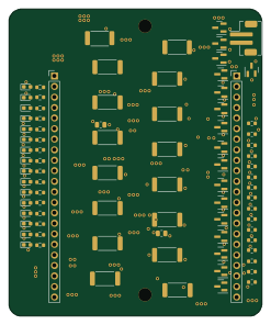
Module 16S PassiveBalanceAddOn
stuartpittaway
61 × 74 mm86 parts2LCC-BY-NC-4.01.1k