
ABSIS Mega

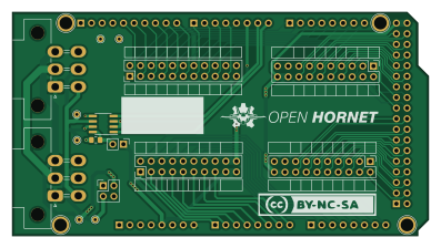
About the ABSIS Mega PCB
ABSIS Mega is an open source PCB design by Exprezz0, published on GitHub under the CC-BY-NC-4.0 license. It is a 2-layer board measuring 99.1 × 53.3 mm, with 10 components from 10 distinct parts.
Other key parts include the MAX487EESA+T. By type, the board carries 7 connectors, 1 IC, 1 jumper and 1 capacitor.
From the project
Based on OpenHornet design - Modified for Personal Use.
The purpose of this guide is to help enable the end-user to successfully accomplish the following: 1: Facilitate navigation of the file structure. 2: Provide clarification regarding the manufacturing process of PCB's related to OpenHornet using JLCPCB.com 2: How to install KiCad 6 and set up libraries associated with OpenHornet. (optional)__
Note: Manufacturing files have been generated accordinging to JLCPCB.com guidelines. If choosing a different PCB Manufacturer, make sure to research their formatting standards and modify the necessary manufacturing files accordingly. And if you choose to…

Main components on the ABSIS Mega
ABSIS Mega bill of materials (BOM)
10 components, 10 distinct parts — part numbers from the project's BOM.
| Qty | Part | Footprint | Refs |
|---|---|---|---|
| 1 | MAX487EESA+T | SOIC-8_3.9x4.9mm_P1.27mm | U1 |
| 1 | BUS IN | Molex_Mini-Fit_Jr_5569-06A1_2x03_P4.20mm_Horizontal | J1 |
| 1 | BUS OUT | Molex_Mini-Fit_Jr_5569-06A1_2x03_P4.20mm_Horizontal | J2 |
| 1 | DIGITAL #1 | PinHeader_2x11_P2.54mm_Vertical | J3 |
| 1 | ANALOG I/O | PinHeader_2x10_P2.54mm_Vertical | J4 |
| 1 | DIGITAL #2 | PinHeader_2x10_P2.54mm_Vertical | J5 |
| 1 | DIGITAL #3 | PinHeader_2x10_P2.54mm_Vertical | J6 |
| 1 | ACC PWR | PinHeader_2x02_P2.54mm_Vertical | J7 |
| 1 | BUS ENABLE | PinHeader_1x02_P2.54mm_Vertical | JP1 |
| 1 | 0.1uF | C_0805_2012Metric_Pad1.15x1.40mm_HandSolder | C1 |
ABSIS Mega design files
The KiCad project lives in the Exprezz0/F-18C_Simulator repository on GitHub; these links point at the commit this page was built from.
ABSIS Mega: common questions
How big is the ABSIS Mega PCB?
The ABSIS Mega measures 99.1 × 53.3 mm, has 2 copper layers and is 1.6 mm thick.
How many components are on the ABSIS Mega?
10 components, from 10 distinct parts, with part numbers taken from the project's own BOM. The full bill of materials is listed on this page.
Where can I download the ABSIS Mega design files?
From the Exprezz0/F-18C_Simulator repository on GitHub, which has the KiCad layout, the schematic and the BOM; the links under Design files point to each one.
Can I use the ABSIS Mega design in my own project?
It is published under CC-BY-NC-4.0, which limits how it may be reused; read the license before building on it.
More boards in F-18C_Simulator
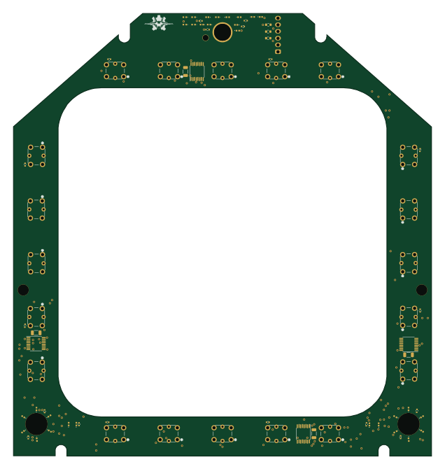
DDI
158.2 × 167.4 mm79 parts2LCC-BY-NC-4.014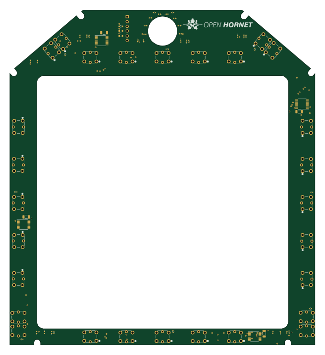
AMPCD
162.9 × 178.9 mm78 parts2LCC-BY-NC-4.014
CONTROLLER Throttle
47 × 68 mm48 parts2LCC-BY-NC-4.014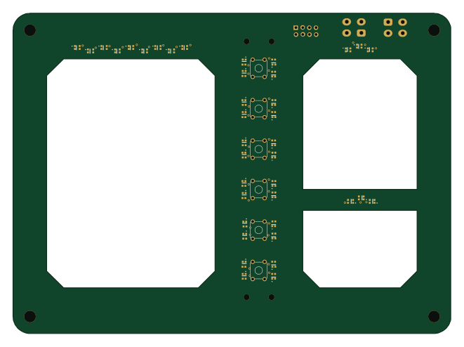
Ifei
165.1 × 120.7 mm45 parts2LCC-BY-NC-4.014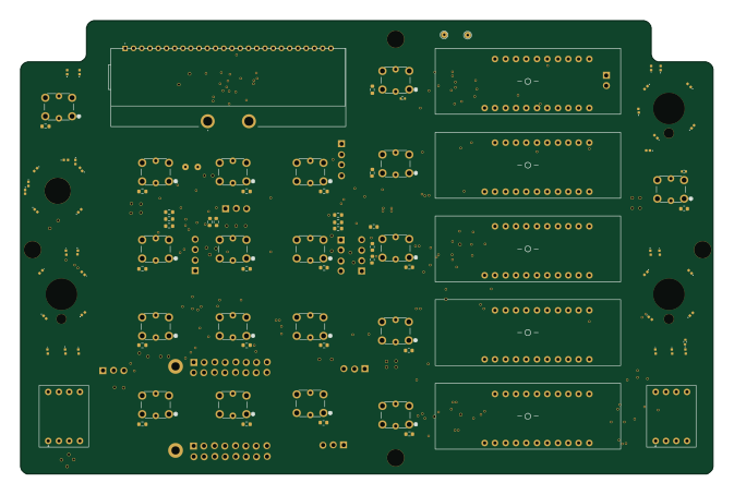
UFC Main
168 × 110 mm44 parts2LCC-BY-NC-4.014
GAUGE Dual Needle Instruments
54.6 × 39.2 mm43 parts4LCC-BY-NC-4.014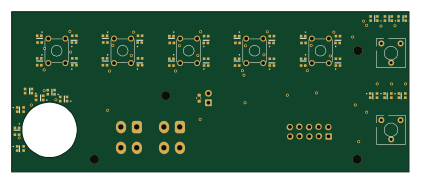
ABSIS NANO GENERAL I/O
105.2 × 42.4 mm41 parts2LCC-BY-NC-4.014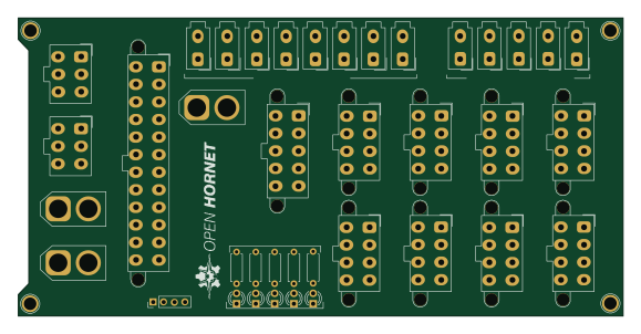
ABSIS ATX Power Supply Unit
144.4 × 71.1 mm39 parts4LCC-BY-NC-4.014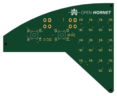
EYEBROW WARNING INDICATOR LEFT
96.1 × 78.8 mm34 parts2LCC-BY-NC-4.014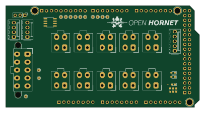
ABSIS Backlight Controller
101.6 × 53.3 mm22 parts2LCC-BY-NC-4.014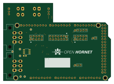 AVR/Arduino
CONTROLLER Standby Instrument
99.1 × 71.1 mm14 parts2LCC-BY-NC-4.014