
Project-LabAnalogDesign2

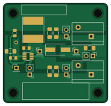
About the Project-LabAnalogDesign2 PCB
Project-LabAnalogDesign2 is an open source PCB design by Fescron, published on GitHub under the CERN-OHL-1.2 license. It is a 2-layer board measuring 40 × 38.1 mm, with 21 components from 15 distinct parts.
Other key parts include the RT8259GE. By type, the board carries 5 test points, 5 capacitors, 3 resistors, 2 connectors, 2 jumpers and 1 IC.
It belongs with the power & battery and dev boards & breakouts designs in this gallery.
From the project
Project-LabAnalogDesign2
The goal of this lab was to design a 5 - 9V to 3,3V (500 mA min) buck converter from the ground up. We had to start from a given chip (RT8259GE) and create the rest ourselves.
Careful layout considerations were taken to lead to an optimal design. The 0Ω resistor is not on the schematic but only on the board layout. It's footprint was used to jump over the feedback track so everything is on the top layer. A via to GND is placed around it as well for redundancy.
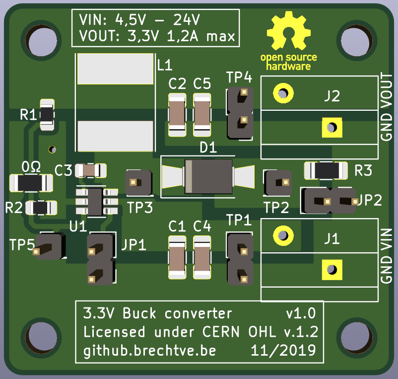
Main components on the Project-LabAnalogDesign2
Project-LabAnalogDesign2 bill of materials (BOM)
21 components, 15 distinct parts.
| Qty | Part | Footprint | Refs |
|---|---|---|---|
| 1 | RT8259GE | SOT-23-6_Handsoldering | U1 |
| 2 | Conn_01x02 | PhoenixContact_PTSA_1,5_2-G-3,5_1x02_P3.50mm_Angled | J1, J2 |
| 1 | R_1206_3216Metric_Pad1.42x1.75mm_HandSolder | R_1206_3216Metric_Pad1.42x1.75mm_HandSolder | 0Ω |
| 1 | Jumper_NO_Small | PinHeader_1x02_P2.54mm_Vertical | JP1 |
| 1 | Jumper_NC_Small | PinHeader_1x02_P2.54mm_Vertical | JP2 |
| 2 | TestPoint_2Pole | PinHeader_1x02_P2.54mm_Vertical | TP1, TP4 |
| 3 | TestPoint | PinHeader_1x01_P2.54mm_Vertical | TP2, TP3, TP5 |
| 1 | D_Schottky_Small_ALT | D_SMA-SMB_Universal_Handsoldering | D1 |
| 1 | 4,7 µH | L_Taiyo-Yuden_NR-80xx_HandSoldering | L1 |
| 2 | 10 µF | C_1206_3216Metric_Pad1.42x1.75mm_HandSolder | C1, C4 |
| 2 | 22 µF | C_1206_3216Metric_Pad1.42x1.75mm_HandSolder | C2, C5 |
| 1 | 10 nF | C_0805_2012Metric_Pad1.15x1.40mm_HandSolder | C3 |
| 1 | 62 kΩ | R_0805_2012Metric_Pad1.15x1.40mm_HandSolder | R1 |
| 1 | 19,6 kΩ | R_0805_2012Metric_Pad1.15x1.40mm_HandSolder | R2 |
| 1 | 0,1 Ω | R_1206_3216Metric_Pad1.42x1.75mm_HandSolder | R3 |
Project-LabAnalogDesign2 design files
The KiCad project lives in the Fescron/Project-LabAnalogDesign2 repository on GitHub; these links point at the commit this page was built from.
Project-LabAnalogDesign2: common questions
How big is the Project-LabAnalogDesign2 PCB?
The Project-LabAnalogDesign2 measures 40 × 38.1 mm, has 2 copper layers and is 1.6 mm thick.
How many components are on the Project-LabAnalogDesign2?
21 components, from 15 distinct parts. The full bill of materials is listed on this page.
Where can I download the Project-LabAnalogDesign2 design files?
From the Fescron/Project-LabAnalogDesign2 repository on GitHub, which has the KiCad layout; the links under Design files point to each one.
Can I use the Project-LabAnalogDesign2 design in my own project?
Yes, under the terms of its CERN-OHL-1.2 license, which Fescron chose for the repository.
Similar boards
EinkPDA screen
TalismanDesign
95 × 54 mm27 parts2LApache-2.02.0k
Stack chan
stack-chan
50 × 50 mm33 parts2LApache-2.01.7k
Display Carrier
AxxAxx
35.6 × 58.2 mm5 parts2LGPL-3.01.7k
88 Pin Vag Breakout
rusefi
142 × 58 mm91 parts2LGPL-3.01.2k
Breakout 60pin EEC-IV
139.7 × 62.2 mm15 parts2LGPL-3.01.2k
Eecv breakout
140.8 × 53.7 mm9 parts4LGPL-3.01.2k