
FUSB302Breakout


About the FUSB302Breakout PCB
FUSB302Breakout is an open source PCB design by Fortinbra, published on GitHub under the MIT license. It is a 2-layer board measuring 21.1 × 23.9 mm, with 11 components from 7 distinct parts.
Other key parts include the FUSB302BMPX. By type, the board carries 6 capacitors, 3 resistors, 1 IC and 1 connector.
It belongs with the power & battery designs in this gallery.
From the project
A minimal breakout board for the FUSB302BMPX — a programmable USB Type-C controller with USB Power Delivery (PD) support from onsemi. The board exposes the chip's I²C interface, interrupt line, and all USB Type-C signals on a 2.54 mm pin header.
A minimal breakout board for the FUSB302BMPX — a programmable USB Type-C controller with USB Power Delivery (PD) support from onsemi. The board exposes the chip's I²C interface, interrupt line, and all USB Type-C signals on a 2.54 mm pin header.
- FUSB302BMPX in WQFN-14 (2.5 × 2.5 mm) package - I²C interface (fixed address 0x22) with 4.7 kΩ pull-up resistors on SDA and SCL - Active-low interrupt line (INT\_N) with pull-up resistor - CC1 and CC2 lines broken out for cable orientation detection and PD communication - VBUS and VCONN pins broken out - Decoupling capacitors on VDD (100 nF + 1 µF)…
Main components on the FUSB302Breakout
FUSB302Breakout bill of materials (BOM)
11 components, 7 distinct parts.
| Qty | Part | Footprint | Refs |
|---|---|---|---|
| 1 | FUSB302BMPX | WQFN-14-1EP_2.5x2.5mm_P0.5mm_EP1.45x1.45mm | U1 |
| 1 | Conn_01x09 | PinHeader_1x09_P2.54mm_Vertical | J3 |
| 2 | 600pf | CP_Radial_D4.0mm_P1.50mm | C1, C2 |
| 2 | 0.1uf | C_0603_1608Metric_Pad1.08x0.95mm_HandSolder | C3, C5 |
| 1 | 1uf | C_0603_1608Metric_Pad1.08x0.95mm_HandSolder | C4 |
| 1 | 220uf | C_1206_3216Metric_Pad1.33x1.80mm_HandSolder | C6 |
| 3 | 4.7k | R_0603_1608Metric_Pad0.98x0.95mm_HandSolder | R1, R2, R3 |
FUSB302Breakout design files
The KiCad project lives in the Fortinbra/FUSB302Breakout repository on GitHub; these links point at the commit this page was built from.
- Layoutsrc/FUSB302Breakout.kicad_pcb
- Schematicsrc/FUSB302Breakout.kicad_sch
FUSB302Breakout: common questions
How big is the FUSB302Breakout PCB?
The FUSB302Breakout measures 21.1 × 23.9 mm, has 2 copper layers and is 1.6 mm thick.
How many components are on the FUSB302Breakout?
11 components, from 7 distinct parts. The full bill of materials is listed on this page.
Where can I download the FUSB302Breakout design files?
From the Fortinbra/FUSB302Breakout repository on GitHub, which has the KiCad layout and the schematic; the links under Design files point to each one.
Can I use the FUSB302Breakout design in my own project?
Yes, under the terms of its MIT license, which Fortinbra chose for the repository.
Similar boards
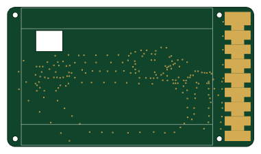
EinkPDA screen
TalismanDesign
95 × 54 mm27 parts2LApache-2.02.0k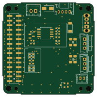
Stack chan
stack-chan
50 × 50 mm33 parts2LApache-2.01.7k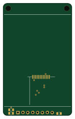
Display Carrier
AxxAxx
35.6 × 58.2 mm5 parts2LGPL-3.01.7k
ProgrammingAdapter
stuartpittaway
10.5 × 83 mm3 parts2LCC-BY-NC-4.01.1k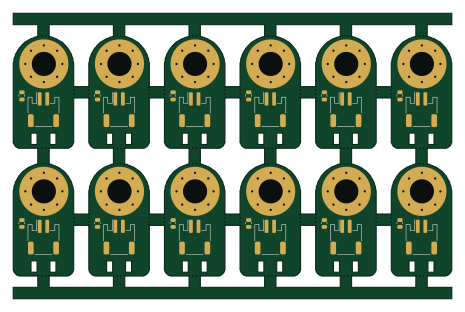
TemperaturePCB PANEL
116 × 75.5 mm178 parts2LCC-BY-NC-4.01.1k
Module 16S PassiveBalanceAddOn
61 × 74 mm86 parts2LCC-BY-NC-4.01.1k