
Modulation dependent carrier level

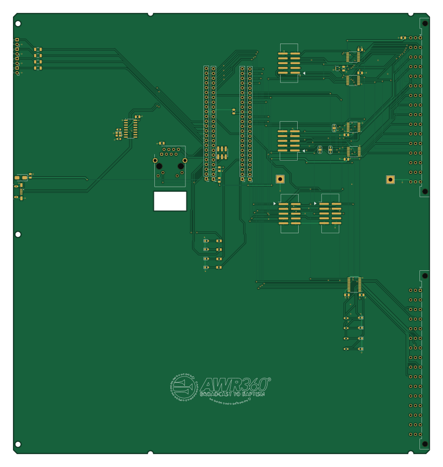
About the Modulation dependent carrier level PCB
Modulation dependent carrier level is an open source NXP PCB design by frohro, published on GitHub under the GPL-3.0 license. It is a 4-layer board measuring 220 × 233 mm, with 64 components from 27 distinct parts.
Its main chip is the C7506622, from the NXP family. Other key parts include the 74LV165, 74AHCT595, C10234, CH340G and SN74LVC8T245. By type, the board carries 16 capacitors, 13 connectors, 13 diodes, 12 resistors, 7 ICs and 2 test points.
From the project
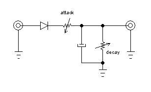
A Modulation Dependent Carrier Level (MDCL) Board for Brown Boveri Shortwave Transmitters
This design should work with any transmitter using an ABB PSM (pulse step modulator) for AM or SW broadcasting designed in the 1980s or 1990s. It replaces the YSE 50 or YSE 21 PCBs in the PSM. I suspect it should work with any transmitter using the YSE 21 or YSE 50. These boards cost around \\$90,000 around the turn of the century, but you should be able to build this one for about $150 each in 2024, the most expensive parts are the DIN connectors that mate the board to the transmitter. These boards are far better, because they use software to do the MDCL and facilitate experimentation and…
Main components on the Modulation dependent carrier level
Modulation dependent carrier level bill of materials (BOM)
64 components, 27 distinct parts — part numbers from the project's BOM.
| Qty | Part | Footprint | Refs |
|---|---|---|---|
| 2 | 74LV165 | TSSOP-16_4.4x5mm_P0.65mm | U1, U2 |
| 2 | 74AHCT595 | TSSOP-16_4.4x5mm_P0.65mm | U3, U4 |
| 1 | C10234 74HC1G04GW,125 | SOT-353_SC-70-5 | U5 |
| 1 | CH340G | SOP-16_3.9x9.9mm_P1.27mm | U6 |
| 1 | SN74LVC8T245 | TSSOP-24_4.4x7.8mm_P0.65mm | U7 |
| 1 | C963522 12 MHz | Crystal_SMD_2520-4Pin_2.5x2.0mm | Y1 |
| 1 | Top DIN | DIN41612_F_3x16_Male_Horizontal_THT | J1 |
| 1 | Lower DIN | DIN41612_F_3x16_Male_Horizontal_THT | J2 |
| 1 | J1B1211CCD | RJ45_Cetus_J1B1211CCD_Horizontal | J3 |
| 1 | C2682512 USB_B_Micro | USB_Micro-Yuandi-G3P3-A1T2 | J4 |
| 1 | C2843214 Logic Analyzer SPI0 | IDC-Header_2x05_P2.54mm_Vertical_SMD | J5 |
| 1 | C2843214 Logic Analyzer D_In | IDC-Header_2x05_P2.54mm_Vertical_SMD | J6 |
| 1 | C2843214 Logic Analyzer D_Out | IDC-Header_2x05_P2.54mm_Vertical_SMD | J7 |
| 2 | C7506622 Teensy socket | PinHeader_1x24_P2.54mm_Vertical | J8, J9 |
| 1 | C2843214 Logic Analyzer SPI1 | IDC-Header_2x05_P2.54mm_Vertical_SMD | J10 |
| 1 | C3975167 Ethernet Jack Socket | PinHeader_2x03_P2.00mm_Vertical_SMD | J11 |
| 2 | Teensy Header | PinHeader_1x24_P2.54mm_Vertical | J12, J13 |
| 2 | GND | TestPoint_THTPad_4.0x4.0mm_Drill2.0mm | TP1, TP2 |
| 1 | SS14 | D_SMA | D1 |
| 4 | HV-32H307B/260/XSYG | LED_3.0mm_2.54mm_lead_spacing_horizontal | D2, D4, D5, D6 |
Show 7 more
| Qty | Part | Footprint | Refs |
|---|---|---|---|
| 8 | LED | LED_0603_1608Metric | D3, D7, D8, D9, D10, D11, D12, D13 |
| 13 | 0.1U 0.1u | C_0805_2012Metric | C1, C2, C4, C5, C6, C7, C8, C9 +5 |
| 2 | 10P 10p | C_0603_1608Metric | C10, C14 |
| 1 | 10U 10u | C_0805_2012Metric | C18 |
| 4 | 470 | R_1206_3216Metric | R1, R2, R3, R4 |
| 4 | 100 | R_0805_2012Metric | R5, R6, R7, R8 |
| 4 | 470 | R_0603_1608Metric | R9, R10, R11, R12 |
Modulation dependent carrier level design files
The KiCad project lives in the frohro/modulation-dependent-carrier-level repository on GitHub; these links point at the commit this page was built from.
Modulation dependent carrier level: common questions
What microcontroller does the Modulation dependent carrier level use?
The Modulation dependent carrier level is built around the C7506622, from the NXP family.
How big is the Modulation dependent carrier level PCB?
The Modulation dependent carrier level measures 220 × 233 mm, has 4 copper layers and is 1.6 mm thick.
How many components are on the Modulation dependent carrier level?
64 components, from 27 distinct parts, with part numbers taken from the project's own BOM. The full bill of materials is listed on this page.
Where can I download the Modulation dependent carrier level design files?
From the frohro/modulation-dependent-carrier-level repository on GitHub, which has the KiCad layout, the schematic and the BOM; the links under Design files point to each one.
Can I use the Modulation dependent carrier level design in my own project?
Yes, under the terms of its GPL-3.0 license, which frohro chose for the repository.
Can I test firmware for the Modulation dependent carrier level without the hardware?
Yes. HardLabs builds a simulation of the board from its netlist and BOM, so you can run and debug NXP firmware against it before you order a PCB.
Similar boards
 NXP
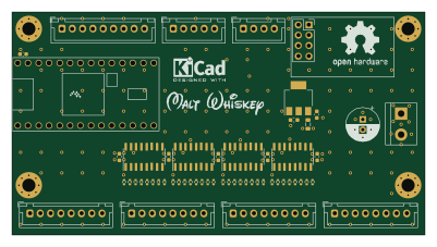
32Bit shift register
MaltWhiskey
100 × 54 mm56 parts4LNo license763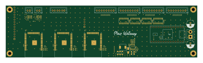 NXP
Mega-Cube-Board
200 × 54 mm100 parts4LNo license763 NXP
MCL6809
MicroCoreLabs
32.3 × 61 mm7 parts4LNo license532 NXP
MCL68
31.6 × 84.1 mm13 parts4LNo license532 NXP
MCL65+
72.6 × 64.1 mm6 parts2LNo license532 NXP
MCLZ8
37.1 × 61.5 mm6 parts4LNo license532