
Bga in two layers

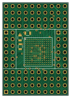
About the Bga in two layers PCB
Bga in two layers is an open source PCB design by google, published on GitHub under the Apache-2.0 license. It is a 2-layer board measuring 25.4 × 35.6 mm, with 23 components from 10 distinct parts.
By type, the board carries 16 capacitors, 4 connectors and 3 resistors.
It belongs with the retro computing designs in this gallery.
From the project
Phillip Pearson's retro hardware projects for the Acorn Electron
An attempt to route a 10M04/10M08 BGA FPGA using only two copper layers. Unfortunately also a test to see how little grounding I can get away with! This should at least let me try to solder and bring up a 10M08 chip, and hopefully the crosstalk at 2MHz won't be so bad.
I'm using the free version of Intel's Quartus Prime software, programming in VHDL.
To program the design into the chip, I generate an .svf file from the Quartus Prime Programmer, then use OpenOCD and my J-Link or Bus Blaster to download it. See openocd.cfg for a working command set.
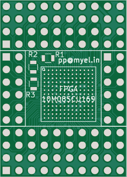
Bga in two layers bill of materials (BOM)
23 components, 10 distinct parts — part numbers from the project's BOM.
| Qty | Part | Footprint | Refs |
|---|---|---|---|
| 1 | top | header_4x10_100mil | CON1 |
| 1 | left | header_2x06_100mil | CON2 |
| 1 | right | header_2x06_100mil | CON3 |
| 1 | bottom | header_4x10_100mil | CON4 |
| 2 | C49678 1u | C_0805 | C8, C9 |
| 6 | C49678 100n | C_0402 | C10, C11, C12, C13, C14, C15 |
| 8 | 100n | C_0402 | C16, C17, C18, C19, C20, C21, C22, C23 |
| 1 | C17414 10k | R_0805 | R1 |
| 1 | C17513 10k | R_0805 | R2 |
| 1 | C17630 1-10k | R_0805 | R3 |
Bga in two layers design files
The KiCad project lives in the google/myelin-acorn-electron-hardware repository on GitHub; these links point at the commit this page was built from.
Bga in two layers: common questions
How big is the Bga in two layers PCB?
The Bga in two layers measures 25.4 × 35.6 mm, has 2 copper layers and is 1.6 mm thick.
How many components are on the Bga in two layers?
23 components, from 10 distinct parts, with part numbers taken from the project's own BOM. The full bill of materials is listed on this page.
Where can I download the Bga in two layers design files?
From the google/myelin-acorn-electron-hardware repository on GitHub, which has the KiCad layout and the BOM; the links under Design files point to each one.
Can I use the Bga in two layers design in my own project?
Yes, under the terms of its Apache-2.0 license, which google chose for the repository.
More boards in myelin-acorn-electron-hardware
Post box usb
92.9 × 45 mm102 parts4LApache-2.059
A3000 ram buffer
167 × 49.4 mm69 parts2LApache-2.059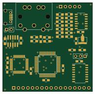
Econet standalone
48.5 × 48 mm67 parts2LApache-2.059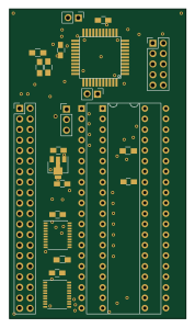
Cpu socket expansion
42.6 × 74.7 mm52 parts2LApache-2.059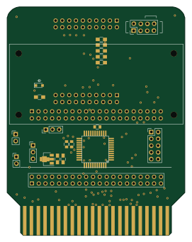 Raspberry Pi
Fx2 tube cartridge adapter
66.5 × 85.5 mm51 parts2LApache-2.059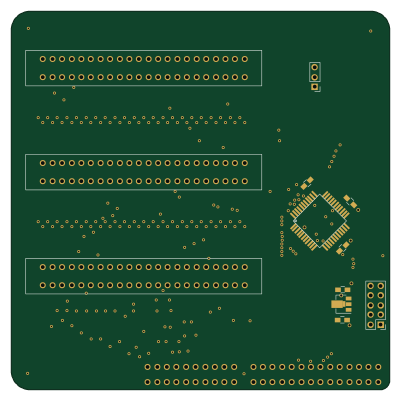
Minus one
100 × 100 mm43 parts2LApache-2.059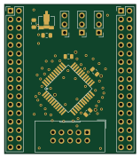
Xc9500xl 44 breakout
39.1 × 44.3 mm29 parts2LApache-2.059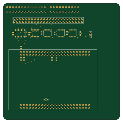
Acorn electron expansion
100 × 100 mm21 parts2LApache-2.059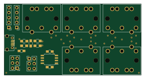
Econet hub
70.7 × 36.6 mm20 parts2LApache-2.059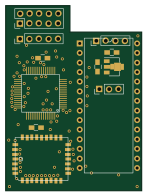
Master updateable megarom
36 × 49 mm18 parts2LApache-2.059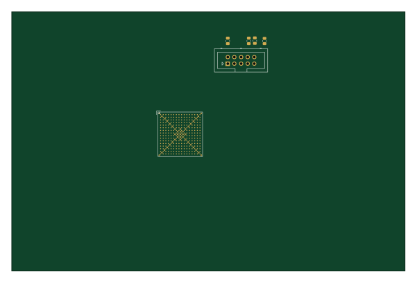
Archimedes bus scope
149.9 × 99.1 mm4 parts4LApache-2.059
Similar boards
OpenTendo
Redherring32
196.3 × 118.7 mm93 parts2LTAPR-OHL-1.0850
24pin flex interposer
Wren6991
29 × 32 mm3 parts2LNo license508
Sram dev board
50 × 50 mm12 parts2LNo license508
GB-BRK-SLOT-A
Gekkio
81 × 80 mm20 parts2LCC-BY-4.0376
GB-BRK-SLOT-B
81 × 80 mm20 parts2LCC-BY-4.0376
GB-BRK-CPU-G2
80 × 80 mm12 parts2LCC-BY-4.0376