
FPGA Logic Analyzer

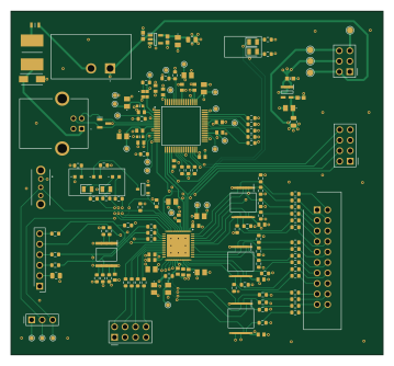
About the FPGA Logic Analyzer PCB
FPGA Logic Analyzer is an open source FPGA PCB design by hack-a-tack, published on GitHub. It is a 4-layer board measuring 89.7 × 82.9 mm, with 144 components from 44 distinct parts.
Its main chip is the ICE40UP5K-SG48I, from the FPGA family. Other key parts include the MIC5504-3.3YM5-TR, MIC5504-1.2YM5-TR, FT2232HL-TRAY, W25Q40CLSNIG and SN74LVC14ADBRE4. By type, the board carries 74 resistors, 38 capacitors, 9 diodes, 8 ICs, 7 connectors and 2 switches.
It belongs with the test & measurement designs in this gallery, and the repository also holds 1 earlier revision of it.
From the project
(NOTE TO SELF: THIS MUST BE UPDATED FOR THE FINAL REVISION; REV1 IS VIRTUALLY IRRELEVANT HERE, ONLY RELEVANT IN REPORT IF USED TO DISCUSS IMPORTANT DESIGN DECISIONS)
(NOTE TO SELF: THIS MUST BE UPDATED FOR THE FINAL REVISION; REV1 IS VIRTUALLY IRRELEVANT HERE, ONLY RELEVANT IN REPORT IF USED TO DISCUSS IMPORTANT DESIGN DECISIONS)
(Info applies to rev. 1, update for later revisions (only final rev. matters in the README)) FPGA-based 8-channel logic analyzer implemented on iCE40UP5K. Supports 24 MHz sampling, 4096 sample depth, UART streaming and trigger logic.
Main components on the FPGA Logic Analyzer
FPGA Logic Analyzer bill of materials (BOM)
144 components, 44 distinct parts — part numbers from the project's BOM.
| Qty | Part | Footprint | Refs |
|---|---|---|---|
| 1 | ICE40UP5K-SG48I | QFN50P700X700X100-49N-D | IC1 |
| 1 | MIC5504-3.3YM5-TR | SOT95P280X145-5N | IC2 |
| 1 | MIC5504-1.2YM5-TR | SOT95P280X145-5N | IC3 |
| 1 | FT2232HL-TRAY | QFP50P1200X1200X160-64N | IC4 |
| 1 | W25Q40CLSNIG | SOIC127P600X175-8N | IC5 |
| 3 | SN74LVC14ADBRE4 | SOP65P780X200-14N | IC6, IC7, IC8 |
| 1 | 2N7002H6327XTSA2 | SOT95P240X110-3N | Q1 |
| 1 | 830208214809 | 830208214809 | Y1 |
| 1 | 61400416121 USB B Female Connector | 61400416121 | J1 |
| 1 | 61300611121 | HDRV6W64P0X254_1X6_1524X254X869P | J2 |
| 1 | 61202021621 | SHDR20W64P254_2X10_3306X910X885P | J3 |
| 2 | 61300821121 Wurth Elektronik | J_Wurth_WR-PHD_61300821121 | J4, J5 |
| 1 | 61300311121 Wurth Elektronik | J_Wurth_WR-PHD_61300311121 | J6 |
| 1 | 61300621121 Wurth Elektronik | J_Wurth_WR-PHD_61300621121 | J7 |
| 1 | 2920L050/72DR 2920L050_72DR | FUSC7451X125N | F1 |
| 1 | BLM21SP601SN1D | BLM21AG102BH1J | FL1 |
| 1 | OS102011MA1QN1 | OS102011MA1QN1 | S1 |
| 1 | L101011MS02Q | L101011MS02Q | S2 |
| 1 | SMAJ5.0A | DIOM5127X229N | D1 |
| 1 | SP0502BAHTG | SOT95P237X112-3N | D2 |
Show 24 more
| Qty | Part | Footprint | Refs |
|---|---|---|---|
| 1 | 150060VS75003 PWR | 150060VS75003 | D3 |
| 1 | 150060VS75003 DONE | 150060VS75003 | D4 |
| 1 | 150060WS75000 USER | 150060WS75000 | D5 |
| 1 | 150080YS75000 TX | LEDC2012X70N | D6 |
| 1 | APT2012LVBC/D RX | LEDC2012X85N | D7 |
| 1 | APT2012LVBC/D FTDI_RX | LEDC2012X85N | D8 |
| 1 | 150080YS75000 FTDI_TX | LEDC2012X70N | D9 |
| 2 | BLM18AG601SN1D | BLM18SP221SN1B | FB1, FB2 |
| 11 | C0805C475K4RACTM 4u7 | C0805 | C1, C12, C15, C17, C20, C21, C22, C23 +3 |
| 4 | MBASE168SB7105KTNA18 1u | INDC1608X90N | C2, C3, C4, C5 |
| 1 | CL10A335KP8NNNC 3u3 | C0805 | C6 |
| 22 | C0603C104M4RACTM 0u1 | CAPC1608X95N | C7, C8, C9, C10, C11, C13, C14, C16 +14 |
| 16 | ERJ-3EKF1002V 10k | R_0603_1608Metric | R1, R3, R8, R9, R10, R15, R18, R19 +8 |
| 1 | ERJ-PC3B1202V 12k | R_0603_1608Metric | R2 |
| 1 | ERJ-PC3B4701V 4k7 | R_0603_1608Metric | R4 |
| 1 | RC0603FR-071KL 1k | R_0603_1608Metric | R5 |
| 6 | CR0603-FX-6800ELF 680R | R_0603_1608Metric | R6, R7, R20, R22, R23, R24 |
| 3 | RC0603JR-0722RL 22R | R_0603_1608Metric | R11, R12, R13 |
| 9 | 560112116009 100R | R_0603_1608Metric | R14, R17, R65, R66, R67, R69, R70, R71 +1 |
| 1 | RC0603FR-07100KL 100k | R_0603_1608Metric | R16 |
| 1 | CR0603-FX-3300ELF 330R | R_0603_1608Metric | R21 |
| 16 | 330R | R_0603_1608Metric | R25, R26, R27, R28, R29, R30, R31, R32 +8 |
| 16 | 100k | R_0603_1608Metric | R41, R42, R43, R44, R45, R46, R47, R48 +8 |
| 3 | RC0805JR-070RL 0R | R_0805_2012Metric | R68, R73, R74 |
FPGA Logic Analyzer design files
The KiCad project lives in the hack-a-tack/FPGA_Logic_Analyzer repository on GitHub; these links point at the commit this page was built from.
FPGA Logic Analyzer: common questions
What microcontroller does the FPGA Logic Analyzer use?
The FPGA Logic Analyzer is built around the ICE40UP5K-SG48I, from the FPGA family.
How big is the FPGA Logic Analyzer PCB?
The FPGA Logic Analyzer measures 89.7 × 82.9 mm, has 4 copper layers and is 1.6 mm thick.
How many components are on the FPGA Logic Analyzer?
144 components, from 44 distinct parts, with part numbers taken from the project's own BOM. The full bill of materials is listed on this page.
Where can I download the FPGA Logic Analyzer design files?
From the hack-a-tack/FPGA_Logic_Analyzer repository on GitHub, which has the KiCad layout, the schematic and the BOM; the links under Design files point to each one.
Can I use the FPGA Logic Analyzer design in my own project?
The repository has no license, so all rights stay with hack-a-tack. Use it as a reference, and ask the author before reusing the design.
Can I test firmware for the FPGA Logic Analyzer without the hardware?
Yes. HardLabs builds a simulation of the board from its netlist and BOM, so you can run and debug FPGA firmware against it before you order a PCB.
Earlier revisions in the repo: iCE40UP5K_logic_analyzer
Similar boards
 FPGA
FPGABase board
GlasgowEmbedded
80 × 49 mm222 parts4L0BSD2.2k FPGA
FPGAThunderscope Rev5.3
EEVengers
122.5 × 103.5 mm817 parts6LMIT1.3k FPGA
FPGAUsb sniffer
ataradov
58.2 × 38.1 mm86 parts2LBSD-3-Clause1.3k FPGA
FPGATomu, I'm
theacodes
13 × 9.4 mm40 parts4LMIT1.1k FPGA
FPGAIcepi zero
cheyao
65 × 30 mm143 parts4LSHL-2.1828 FPGA
FPGASd2snes
mrehkopf
101.5 × 83 mm147 partsGPL-2.0717