
Rp2040 usbc panel

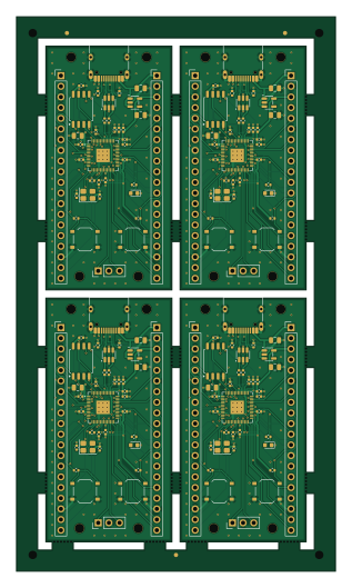
About the Rp2040 usbc panel PCB
Rp2040 usbc panel is an open source RP2040/RP2350 PCB design by haiha-ux, published on GitHub. It is a 4-layer board measuring 76 × 132 mm, with 37 components from 20 distinct parts.
Its main chip is the RP2040, from the RP2040/RP2350 family. Other key parts include the AP2112K-3.3TRG1, W25Q128JVSIQ and USBLC6-2SC6. By type, the board carries 17 capacitors, 8 resistors, 4 ICs, 4 connectors, 2 switches and 1 crystal.
From the project
RP2040 USB-C board, KiCad 10, JLC 4-layer stackup, 90 ohm USB pair, 2x2 panel with DFM check
Owner: Ha Phan Thanh Hai (GitHub haiha-ux). A small RP2040 development board in KiCad 10, laid out for the JLCPCB 4-layer stackup JLC04161H-7628, with fabrication and assembly files and a 2x2 panel. The board is 30 × 58 mm and has a USB-C device port, 16 MB QSPI flash, a 3.3 V LDO, BOOTSEL and RESET buttons, a 3-pin SWD header, a status LED on GPIO25 and two 1x20 headers that bring out GPIO0 to GPIO29.
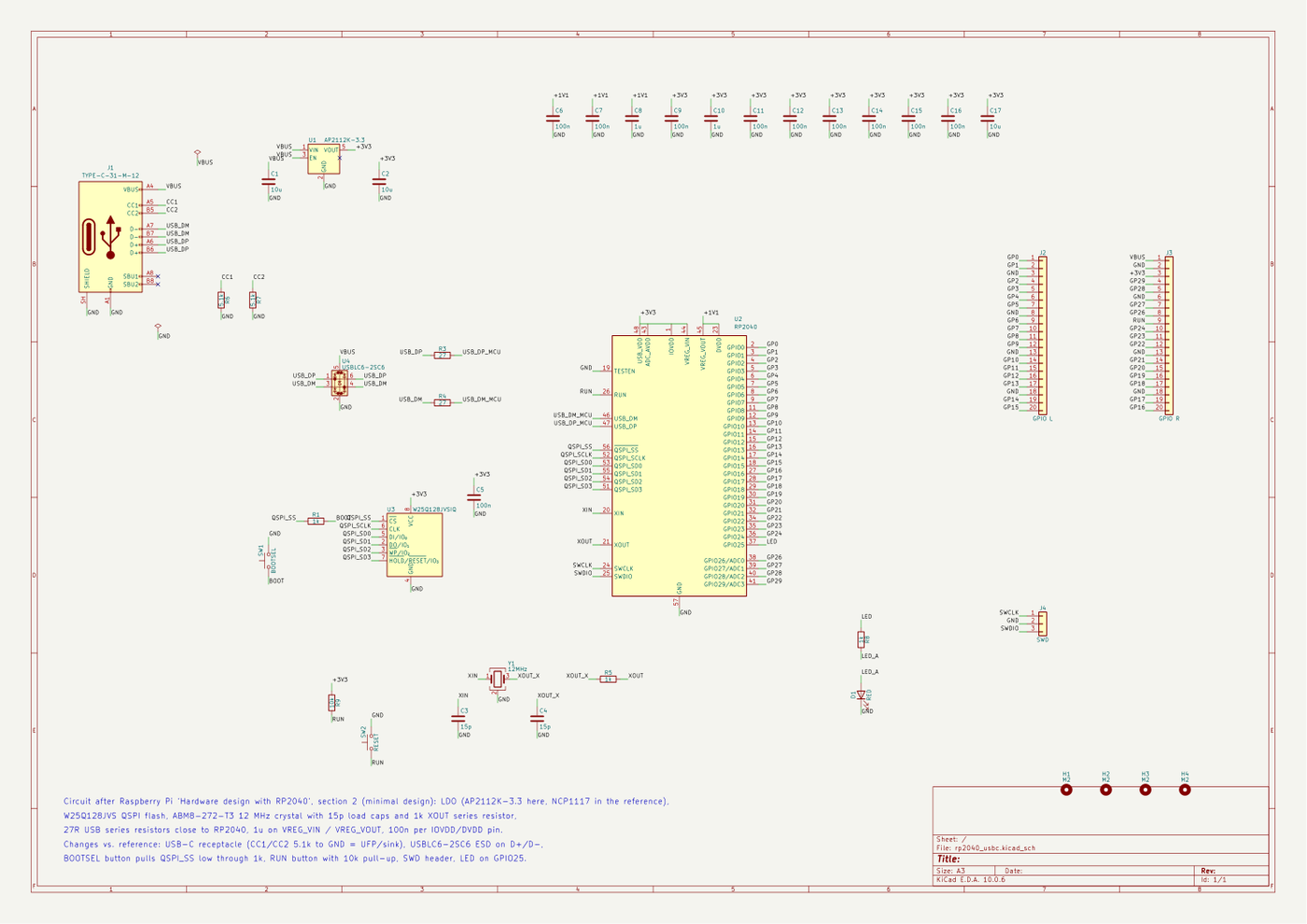
Main components on the Rp2040 usbc panel
Rp2040 usbc panel bill of materials (BOM)
37 components, 20 distinct parts — part numbers from the project's BOM.
| Qty | Part | Footprint | Refs |
|---|---|---|---|
| 1 | AP2112K-3.3TRG1 AP2112K-3.3 Diodes Incorporated | SOT-23-5 | U1 |
| 1 | RP2040 Raspberry Pi | QFN-56-1EP_7x7mm_P0.4mm_EP3.2x3.2mm | U2 |
| 1 | W25Q128JVSIQ Winbond | SOIC-8_5.3x5.3mm_P1.27mm | U3 |
| 1 | USBLC6-2SC6 STMicroelectronics | SOT-23-6 | U4 |
| 1 | ABM8-272-T3 12MHz Abracon | Crystal_SMD_3225-4Pin_3.2x2.5mm | Y1 |
| 1 | TYPE-C-31-M-12 Korean Hroparts Elec | USB_C_Receptacle_HRO_TYPE-C-31-M-12 | J1 |
| 1 | 2.54-1*20PStraight pin GPIO L BOOMELE | PinHeader_1x20_P2.54mm_Vertical | J2 |
| 1 | 2.54-1*20PStraight pin GPIO R BOOMELE | PinHeader_1x20_P2.54mm_Vertical | J3 |
| 1 | 22284030 SWD Molex | PinHeader_1x03_P2.54mm_Vertical | J4 |
| 1 | TS-1187A-B-A-B BOOTSEL XKB Connection | SW_Push_1P1T_XKB_TS-1187A | SW1 |
| 1 | TS-1187A-B-A-B RESET XKB Connection | SW_Push_1P1T_XKB_TS-1187A | SW2 |
| 1 | KT-0603R RED Hubei KENTO Elec | LED_0603_1608Metric | D1 |
| 3 | CL21A106KAYNNNE 10u Samsung Electro-Mechanics | C_0805_2012Metric | C1, C2, C17 |
| 2 | 0402CG150J500NT 15p FH | C_0402_1005Metric | C3, C4 |
| 10 | CL05B104KO5NNNC 100n Samsung Electro-Mechanics | C_0402_1005Metric | C5, C6, C7, C9, C11, C12, C13, C14 +2 |
| 2 | CL05A105KA5NQNC 1u Samsung Electro-Mechanics | C_0402_1005Metric | C8, C10 |
| 3 | 0402WGF1001TCE 1k UNI-ROYAL | R_0402_1005Metric | R1, R5, R8 |
| 2 | FRC0402F27R0TS 27 FOJAN | R_0402_1005Metric | R3, R4 |
| 2 | 0402WGF5101TCE 5.1k UNI-ROYAL | R_0402_1005Metric | R6, R7 |
| 1 | 0402WGF1002TCE 10k UNI-ROYAL | R_0402_1005Metric | R9 |
Rp2040 usbc panel design files
The KiCad project lives in the haiha-ux/pcb-rp2040-usbc repository on GitHub; these links point at the commit this page was built from.
Rp2040 usbc panel: common questions
What microcontroller does the Rp2040 usbc panel use?
The Rp2040 usbc panel is built around the RP2040, from the RP2040/RP2350 family.
How big is the Rp2040 usbc panel PCB?
The Rp2040 usbc panel measures 76 × 132 mm, has 4 copper layers and is 1.6 mm thick.
How many components are on the Rp2040 usbc panel?
37 components, from 20 distinct parts, with part numbers taken from the project's own BOM. The full bill of materials is listed on this page.
Where can I download the Rp2040 usbc panel design files?
From the haiha-ux/pcb-rp2040-usbc repository on GitHub, which has the KiCad layout and the BOM; the links under Design files point to each one.
Can I use the Rp2040 usbc panel design in my own project?
The repository has no license, so all rights stay with haiha-ux. Use it as a reference, and ask the author before reusing the design.
Can I test firmware for the Rp2040 usbc panel without the hardware?
Yes. HardLabs builds a simulation of the board from its netlist and BOM, so you can run and debug RP2040/RP2350 firmware against it before you order a PCB.
More boards in pcb-rp2040-usbc
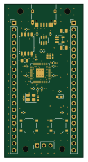
Similar boards
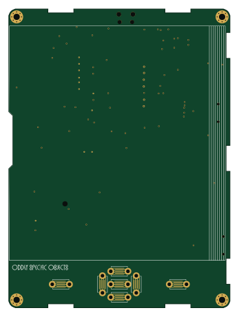 RP2040/RP2350
OSO-BOOK-C1
joeycastillo
85 × 115 mm29 parts2LCC-BY-SA-4.08.1k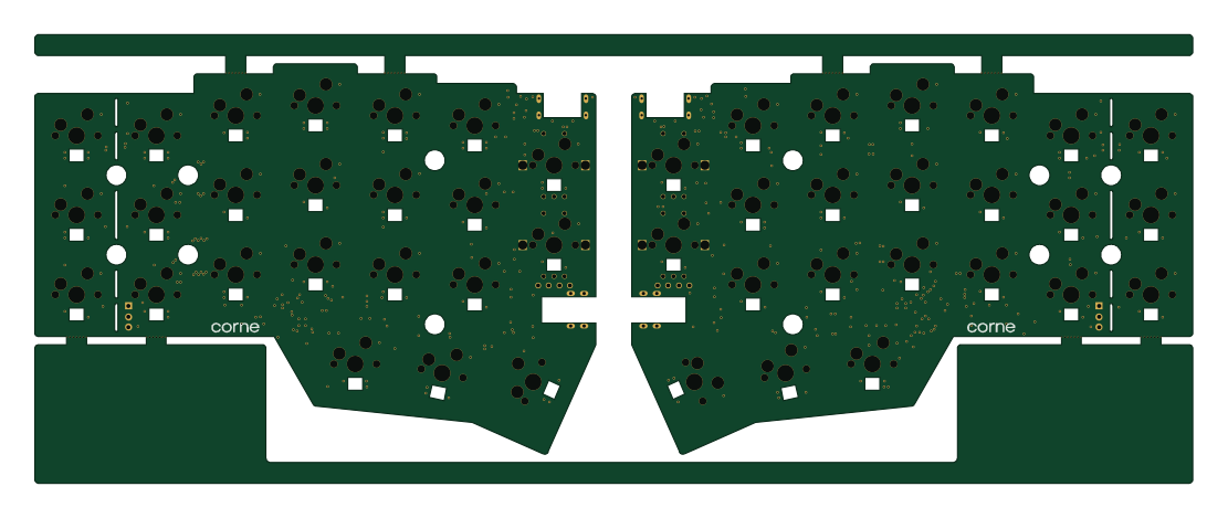 RP2040/RP2350
Corne cherry
foostan
277.2 × 107.5 mm164 parts2LCC-BY-4.07.7k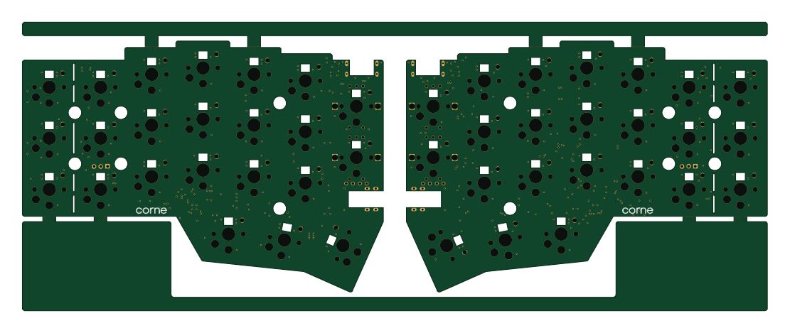 RP2040/RP2350
Corne chocolate
277.2 × 107.5 mm164 parts2LCC-BY-4.07.7k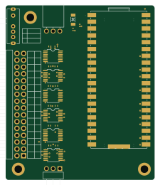 RP2040/RP2350
Jitx design
gusmanb
55.5 × 65 mm26 parts4LGPL-3.05.0k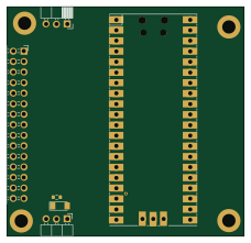 RP2040/RP2350
LogicAnalyzer
57 × 55.2 mm6 parts2LGPL-3.05.0k RP2040/RP2350
Main
google
98 × 71 mm102 parts2LApache-2.02.9k