
OBC-Attempt-2 Matcha 2 Layer 1

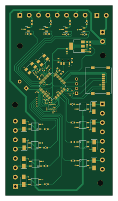
About the OBC-Attempt-2 Matcha 2 Layer 1 PCB
OBC-Attempt-2 Matcha 2 Layer 1 is an open source STM32 PCB design by HelloItzAlex, published on GitHub. It is a 2-layer board measuring 57.2 × 101.6 mm, with 71 components from 30 distinct parts.
Its main chip is the STM32F401RDTx, from the STM32 family. Other key parts include the BMI088, CPC1020NTR and NCP1117-3.3_SOT223. By type, the board carries 19 resistors, 18 capacitors, 11 ICs, 8 diodes, 7 connectors and 4 transistors.
Main components on the OBC-Attempt-2 Matcha 2 Layer 1
OBC-Attempt-2 Matcha 2 Layer 1 bill of materials (BOM)
71 components, 30 distinct parts — part numbers from the project's BOM.
| Qty | Part | Footprint | Refs |
|---|---|---|---|
| 1 | BMI088 | BMI088 | U1 |
| 8 | CPC1020NTR | 4-SOP | U2, U3, U4, U5, U7, U8, U10, U11 |
| 1 | STM32F401RDTx | LQFP-64_10x10mm_P0.5mm | U9 |
| 1 | NCP1117-3.3_SOT223 | SOT-223-3_TabPin2 | U12 |
| 4 | FQP27P06 2N7002K | SOT-23 | Q1, Q2, Q3, Q4 |
| 1 | ABMM2-25MHZ-D1-T | XTAL_ABMM2-25.000MHZ-D1-T | Y1 |
| 1 | ABMM2-32.768MHZ-E2F-T | XTAL_ABMM2-32.768MHZ-E2F-T | Y2 |
| 1 | NI9205CONN Screw_Terminal_01x08 | TerminalBlock_Phoenix_MKDS-1,5-8_1x08_P5.00mm_Horizontal | J1 |
| 1 | Screw_Terminal_01x08 | TerminalBlock_Phoenix_MKDS-1,5-8_1x08_P5.00mm_Horizontal | J2 |
| 1 | 24VCONN Screw_Terminal_01x08 | TerminalBlock_Phoenix_MKDS-1,5-8_1x08_P5.00mm_Horizontal | J3 |
| 1 | Conn_01x04 | PinHeader_1x04_P2.54mm_Vertical | J5 |
| 1 | 24VCONN Micro_SD_Card | microSD_HC_Wuerth_693072010801 | J6 |
| 2 | Screw_Terminal_01x02 | TerminalBlock_Phoenix_MKDS-1,5-2_1x02_P5.00mm_Horizontal | J7, J8 |
| 1 | Buzzer | Buzzer_TDK_PS1240P02BT_D12.2mm_H6.5mm | BZ1 |
| 1 | PCM12SMTR | SW_PCM12SMTR | SW1 |
| 4 | B330 | D_SMA | D1, D2, D3, D4 |
| 4 | 1N4004 B330 | D_SMA | D5, D6, D7, D8 |
| 9 | 100nF | C_0402_1005Metric | C1, C2, C3, C4, C6, C8, C9, C11 +1 |
| 1 | 4.7uF | C_0402_1005Metric | C7 |
| 1 | 1uF | C_0603_1608Metric | C10 |
Show 10 more
| Qty | Part | Footprint | Refs |
|---|---|---|---|
| 4 | 26pf | C_0402_1005Metric | C14, C16, C17, C18 |
| 1 | 4.7uF | C_0603_1608Metric | C15 |
| 1 | 100nF | C_0603_1608Metric | C20 |
| 1 | 10uF | C_0603_1608Metric | C21 |
| 4 | 1.1K 1 | R_0603_1608Metric | R1, R2, R3, R4 |
| 4 | 100K 470 | R_0603_1608Metric | R5, R6, R7, R8 |
| 8 | 100K 270 | R_0603_1608Metric | R9, R10, R11, R12, R14, R15, R16, R17 |
| 1 | 1.1K 10k | R_0603_1608Metric | R13 |
| 1 | 100K 1M | R_0603_1608Metric | R18 |
| 1 | 100K | R_0603_1608Metric | R19 |
OBC-Attempt-2 Matcha 2 Layer 1 design files
The KiCad project lives in the HelloItzAlex/KiCAD-Designs repository on GitHub; these links point at the commit this page was built from.
OBC-Attempt-2 Matcha 2 Layer 1: common questions
What microcontroller does the OBC-Attempt-2 Matcha 2 Layer 1 use?
The OBC-Attempt-2 Matcha 2 Layer 1 is built around the STM32F401RDTx, from the STM32 family.
How big is the OBC-Attempt-2 Matcha 2 Layer 1 PCB?
The OBC-Attempt-2 Matcha 2 Layer 1 measures 57.2 × 101.6 mm, has 2 copper layers and is 1.6 mm thick.
How many components are on the OBC-Attempt-2 Matcha 2 Layer 1?
71 components, from 30 distinct parts, with part numbers taken from the project's own BOM. The full bill of materials is listed on this page.
Where can I download the OBC-Attempt-2 Matcha 2 Layer 1 design files?
From the HelloItzAlex/KiCAD-Designs repository on GitHub, which has the KiCad layout, the schematic and the BOM; the links under Design files point to each one.
Can I use the OBC-Attempt-2 Matcha 2 Layer 1 design in my own project?
The repository has no license, so all rights stay with HelloItzAlex. Use it as a reference, and ask the author before reusing the design.
Can I test firmware for the OBC-Attempt-2 Matcha 2 Layer 1 without the hardware?
Yes. HardLabs builds a simulation of the board from its netlist and BOM, so you can run and debug STM32 firmware against it before you order a PCB.
More boards in KiCAD-Designs
NI-9205 Breakout v2.0
190.5 × 279.4 mm193 parts2LNo license1
2025-2026 NI Breakout Board
190.5 × 279.4 mm193 parts2LNo license1 ESP32
ESP32Constellation Stack V3.0
57.2 × 57.2 mm67 parts4LNo license1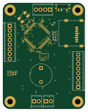 STM32
STM32OBC-Attempt-1 Matcha 4 Layer
44.5 × 57.2 mm65 parts4LNo license1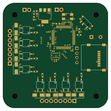 STM32
STM32OBC-Attempt-5 Matcha 2 Layer 3
57.2 × 57.2 mm55 parts2LNo license1 STM32
STM32DeploymentBoardV2.0
20.3 × 31.8 mm46 parts4LNo license1 STM32
STM32Memory Board
29.9 × 38.1 mm34 parts4LNo license1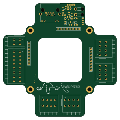
Constellation Saddle V1.2
95.3 × 95.3 mm29 parts2LNo license1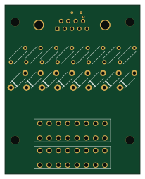
AGS Solenoid Breakout D9
50.8 × 63.5 mm18 parts2LNo license1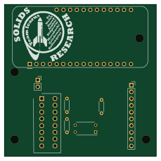
Load Cell Ground Systems
57.2 × 57.2 mm8 parts2LNo license1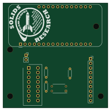
Load Cell Ground Systems STM32
57.2 × 57.2 mm8 parts2LNo license1
Similar boards
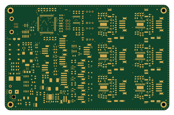 STM32
STM32LumenPnP Motherboard
opulo-inc
149 × 95 mm296 parts4LCC-BY-SA-4.03.7k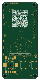 STM32
STM32AxxSolder
AxxAxx
39 × 82.5 mm122 parts2LGPL-3.01.7k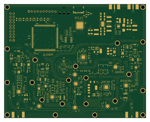 STM32
STM32LibreVNA
jankae
122 × 98 mm592 parts6LGPL-3.01.6k STM32
STM32AIOC
skuep
21 × 31.5 mm47 parts2LMIT1.4k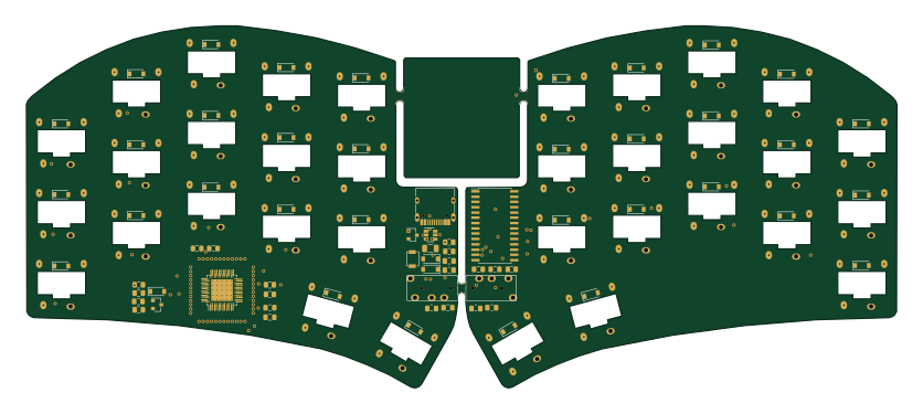 STM32
STM32Ferris
pierrechevalier83
208.8 × 86.8 mm102 parts2LSHL-2.11.3k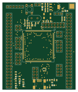 STM32
STM32176 pin board
rusefi
61.8 × 73.2 mm76 parts2LGPL-3.01.2k