
Hackpad for editing

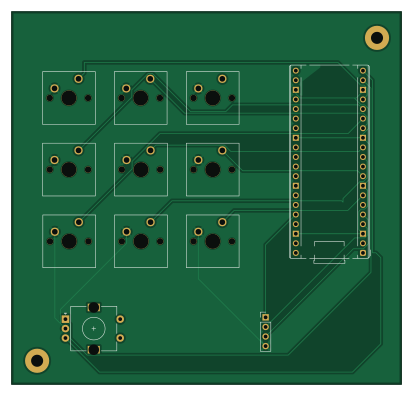
About the Hackpad for editing PCB
Hackpad for editing is an open source RP2040/RP2350 PCB design by heyy-Shubham, published on GitHub under the MIT license. It is a 2-layer board measuring 103.2 × 98.7 mm, with 12 components from 4 distinct parts.
Its main chip is the RaspberryPi_Pico, from the RP2040/RP2350 family. By type, the board carries 10 switches, 1 module and 1 connector.
It belongs with the keyboards, audio and displays & leds designs in this gallery.
From the project
Hackpad for Editing is a custom-built, open-source mechanical macropad designed to supercharge your video and audio editing workflow. It combines a hand-designed PCB schematic (KiCad), a 3D-printed enclosure, and lightweight C++ firmware — all built from scratch. The firmware runs on PlatformIO inside VS Code, making it easy to modify, build, and f
As a video editor, I was tired of reaching across the keyboard for shortcuts like Undo, Redo, and Zoom constantly. I wanted a dedicated device that keeps my hands in the editing zone — so I built the Hackpad For Editing.
I will make this device using 9 swcherrymx (switch) and encoder and 0.91 oled display just plug and enhance editing leval build for editors
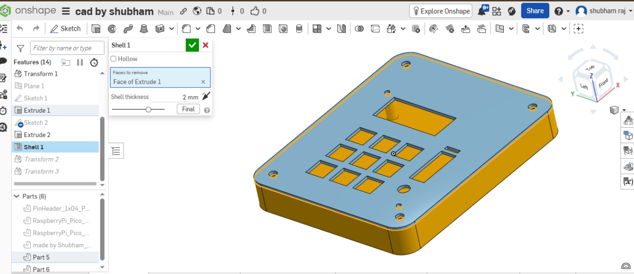
Main components on the Hackpad for editing
Hackpad for editing bill of materials (BOM)
12 components, 4 distinct parts — part numbers from the project's BOM.
| Qty | Part | Footprint | Refs |
|---|---|---|---|
| 1 | RaspberryPi_Pico | RaspberryPi_Pico_Common_THT | A1 |
| 1 | Conn_01x04_Pin | PinHeader_1x04_P2.54mm_Vertical | J1 |
| 9 | SW_SPST | SW_Cherry_MX_1.00u_PCB | SW1, SW2, SW3, SW04, SW5, SW6, SW07, SW8 +1 |
| 1 | RotaryEncoder | RotaryEncoder_Alps_EC11E-Switch_Vertical_H20mm | SW10 |
Hackpad for editing design files
The KiCad project lives in the heyy-Shubham/hackpad-for-editing repository on GitHub; these links point at the commit this page was built from.
Hackpad for editing: common questions
What microcontroller does the Hackpad for editing use?
The Hackpad for editing is built around the RaspberryPi_Pico, from the RP2040/RP2350 family.
How big is the Hackpad for editing PCB?
The Hackpad for editing measures 103.2 × 98.7 mm, has 2 copper layers and is 1.6 mm thick.
How many components are on the Hackpad for editing?
12 components, from 4 distinct parts, with part numbers taken from the project's own BOM. The full bill of materials is listed on this page.
Where can I download the Hackpad for editing design files?
From the heyy-Shubham/hackpad-for-editing repository on GitHub, which has the KiCad layout, the schematic and the BOM; the links under Design files point to each one.
Can I use the Hackpad for editing design in my own project?
Yes, under the terms of its MIT license, which heyy-Shubham chose for the repository.
Can I test firmware for the Hackpad for editing without the hardware?
Yes. HardLabs builds a simulation of the board from its netlist and BOM, so you can run and debug RP2040/RP2350 firmware against it before you order a PCB.
Similar boards
 RP2040/RP2350
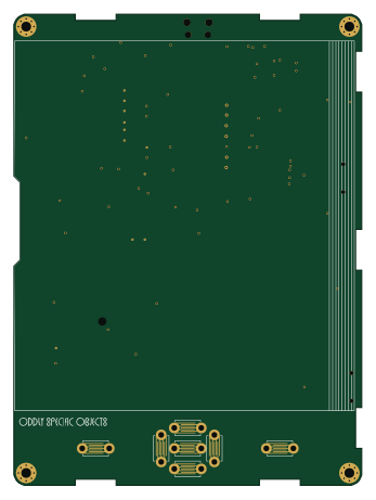
Open Book Abridged Edition
joeycastillo
85 × 115 mm29 parts2LCC-BY-SA-4.08.1k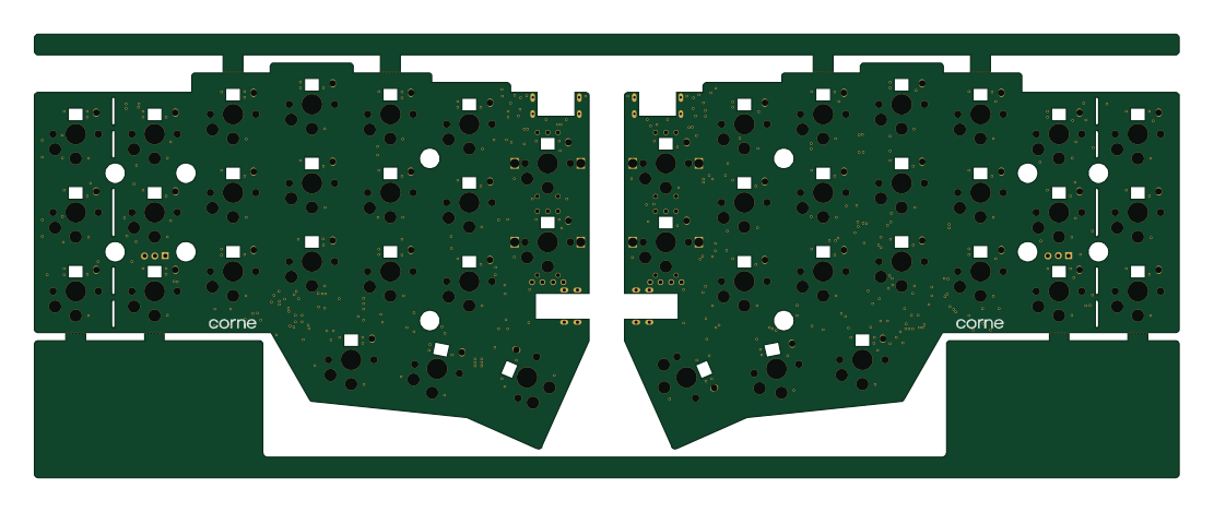 RP2040/RP2350
Corne
foostan
277.2 × 107.5 mm164 parts2LCC-BY-4.07.7k RP2040/RP2350
Corne
277.2 × 107.5 mm164 parts2LCC-BY-4.07.7k RP2040/RP2350
LogicAnalyzer
gusmanb
57 × 55.2 mm6 parts2LGPL-3.05.0k RP2040/RP2350
Jitx design
55.5 × 65 mm26 parts4LGPL-3.05.0k RP2040/RP2350
Pro V2
kata0510
290.1 × 130 mm270 parts2LMIT2.3k