
Hwde led test


About the Hwde led test PCB
Hwde led test is an open source PCB design by Hive-RSI-Lab, published on GitHub under the MIT license. It is a 2-layer board measuring 13.4 × 10.5 mm, with 4 components from 4 distinct parts.
By type, the board carries 1 connector, 1 diode, 1 capacitor and 1 resistor.
From the project
pcb-flow: KiCad PCB design from a written brief to a fab package, as a Hive module (formerly hwde).
A tiny test board that lights one green LED from 5 V. It was the first board the Hive designed with the hwde module, on 2026-10-28, to prove the pipeline runs from brief to checked fab files inside the Hive. It hasn't been ordered. Ordering is the person's call.
- 2 layers, 1.6 mm FR-4, HASL, 13.4 x 10.5 mm, no mounting holes. - J1: a 2-pin 2.54 mm header. Pin 1 (square, marked +) is +5V and pin 2 (marked −) is GND. Use 4.75–5.25 V from a bench supply or a USB 5 V lead. - C1: 4.7 µF 16 V X5R 0603 across the input, next to J1. - R1 + D1: a 470 Ω resistor feeds a green 0603 LED (KT-0603G). The…
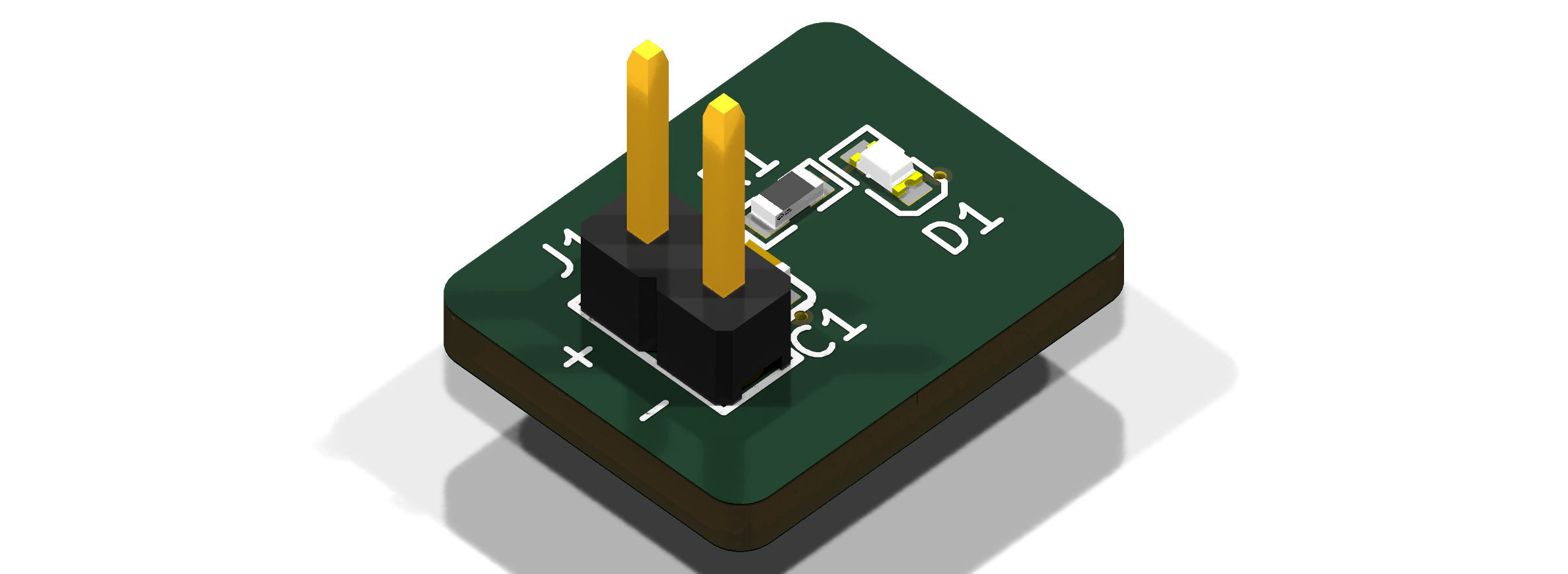
Hwde led test bill of materials (BOM)
4 components, 4 distinct parts — part numbers from the project's BOM.
| Qty | Part | Footprint | Refs |
|---|---|---|---|
| 1 | PZ254V-11-02P | HDR-TH_2P-P2.54-V-M | J1 |
| 1 | KT-0603G | LED0603-RD | D1 |
| 1 | CL10A475KO8NNNC 4.7uF | C0603 | C1 |
| 1 | 0603WAF4700T5E 470R | R0603 | R1 |
Hwde led test design files
The KiCad project lives in the Hive-RSI-Lab/hive-pcb-flow repository on GitHub; these links point at the commit this page was built from.
Hwde led test: common questions
How big is the Hwde led test PCB?
The Hwde led test measures 13.4 × 10.5 mm, has 2 copper layers and is 1.6 mm thick.
How many components are on the Hwde led test?
4 components, from 4 distinct parts, with part numbers taken from the project's own BOM. The full bill of materials is listed on this page.
Where can I download the Hwde led test design files?
From the Hive-RSI-Lab/hive-pcb-flow repository on GitHub, which has the KiCad layout, the schematic and the BOM; the links under Design files point to each one.
Can I use the Hwde led test design in my own project?
Yes, under the terms of its MIT license, which Hive-RSI-Lab chose for the repository.
More boards in hive-pcb-flow
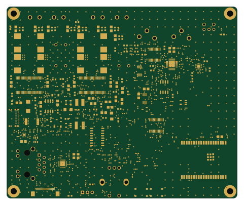 ESP32
Core
120 × 100 mm297 parts4LMIT1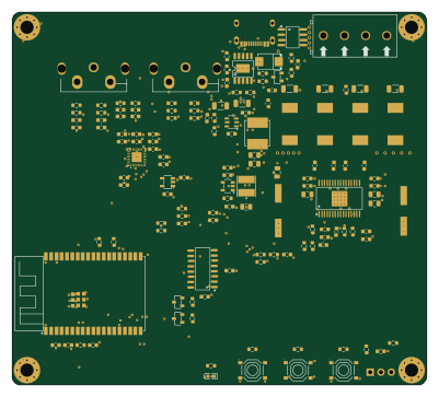 ESP32
Lite main
100 × 90 mm145 parts2LMIT1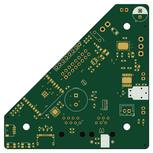 ESP32
Minuet Fan Controller
79 × 79 mm76 parts2LMIT1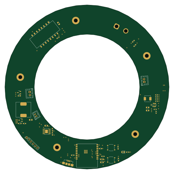 ESP32
Terrarium Control Board
140 × 140 mm51 parts2LMIT1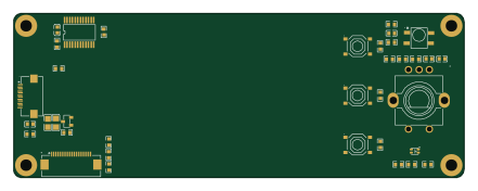
Pre route
110 × 40 mm36 parts2LMIT1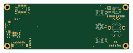
Post route
110 × 40 mm36 parts2LMIT1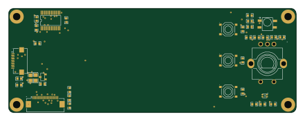
Ultra front
110 × 40 mm36 parts2LMIT1
Post route auto
110 × 40 mm36 parts2LMIT1 RP2040/RP2350
Digits
76.2 × 56.9 mm19 parts2LMIT1