
Typepak advance

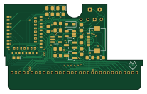
About the Typepak advance PCB
Typepak advance is an open source PCB design by ImStuBTW, published on GitHub under the MIT license. It is a 2-layer board measuring 51.7 × 32 mm, with 25 components from 20 distinct parts.
Other key parts include the E73-2G4M08S1C, AP2112K-3.3 and TP4054. By type, the board carries 7 resistors, 4 connectors, 3 ICs, 3 diodes, 3 capacitors and 2 transistors.
It belongs with the dev boards & breakouts, retro computing and keyboards designs in this gallery.
From the project
An nRF52840 breakout board enclosed in a Game Boy Advance cartridge.
The TypePak Advance is an update to my original TypePak design from 2023. The original idea for the concept was to put as many wireless keyboard components as possible inside of the shell of a Game Boy Advance cartridge. This allows you to more easily move the microcontroller between builds, but honestly it's primarily done for aesthetic reasons. Slapping a Game Boy cartridge port and cartridge onto the side of one's keyboard takes up a decent amount of space compared to a Pro Micro or a XIAO microcontroller, but it does look neat. If you're iterating through designs rapidly, it does manage…
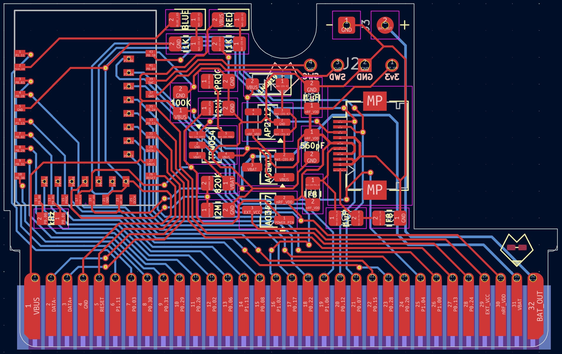
Main components on the Typepak advance
Typepak advance bill of materials (BOM)
25 components, 20 distinct parts.
| Qty | Part | Footprint | Refs |
|---|---|---|---|
| 1 | E73-2G4M08S1C | E73-2G4M08S1C-52840 | U1 |
| 1 | AP2112K-3.3 | SOT-23-5_HandSoldering | U2 |
| 1 | TP4054 | SOT-23-5_HandSoldering | U3 |
| 2 | AO3407 | SOT-23_Handsoldering | Q1, Q2 |
| 1 | 32768kHz | Crystal_SMD_MicroCrystal_CM9V-T1A-2Pin_1.6x1.0mm_HandSoldering | X1 |
| 1 | Conn_01x04 | connector_swd | J2 |
| 1 | Conn_01x02 | SolderWire-0.1sqmm_1x02_P3.6mm_D0.4mm_OD1mm | J3 |
| 1 | Conn_01x32_Pin | GameBoy_GamePak_AGB-002_P1.50mm_Edge | J5 |
| 1 | Conn_01x10 | Hirose_FH12-10S-0.5SH_1x10-1MP_P0.50mm_Horizontal | J6 |
| 1 | 1N5819 | D_SOD-123F | D1 |
| 1 | BLUE | LED_0805_2012Metric_Pad1.15x1.40mm_HandSolder | D2 |
| 1 | RED | LED_0805_2012Metric_Pad1.15x1.40mm_HandSolder | D3 |
| 2 | FerriteBead_Small | R_0805_2012Metric_Pad1.20x1.40mm_HandSolder | FB1, FB2 |
| 1 | 560pF/680pF | C_0805_2012Metric_Pad1.18x1.45mm_HandSolder | C1 |
| 2 | 1uF | C_0805_2012Metric_Pad1.18x1.45mm_HandSolder | C2, C3 |
| 1 | 100K | R_0805_2012Metric_Pad1.20x1.40mm_HandSolder | R1 |
| 2 | 1K | R_0805_2012Metric_Pad1.20x1.40mm_HandSolder | R4, R8 |
| 1 | RPROG | R_0805_2012Metric_Pad1.20x1.40mm_HandSolder | R5 |
| 1 | 820K | R_0805_2012Metric_Pad1.20x1.40mm_HandSolder | R6 |
| 2 | 2M | R_0805_2012Metric_Pad1.20x1.40mm_HandSolder | R7, R9 |
Typepak advance design files
The KiCad project lives in the ImStuBTW/typepak-advance repository on GitHub; these links point at the commit this page was built from.
- Layouttypepak-advance.kicad_pcb
- Schematictypepak-advance.kicad_sch
Typepak advance: common questions
How big is the Typepak advance PCB?
The Typepak advance measures 51.7 × 32 mm, has 2 copper layers and is 1.6 mm thick.
How many components are on the Typepak advance?
25 components, from 20 distinct parts. The full bill of materials is listed on this page.
Where can I download the Typepak advance design files?
From the ImStuBTW/typepak-advance repository on GitHub, which has the KiCad layout and the schematic; the links under Design files point to each one.
Can I use the Typepak advance design in my own project?
Yes, under the terms of its MIT license, which ImStuBTW chose for the repository.
Similar boards
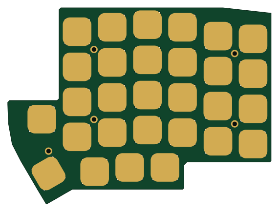
Lily58 Lite Rev3 TOP Case
kata0510
142.5 × 106.4 mm34 parts2LMIT2.3k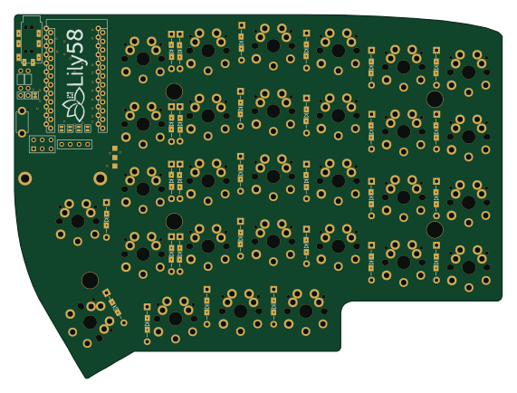
Lily58
142.5 × 106.3 mm83 parts2LMIT2.3k
Lily58 Pro BOTTOM
142.5 × 106.3 mm5 parts2LMIT2.3k
Lily58 Pro
142.5 × 106.3 mm83 parts2LMIT2.3k
KLOR
GEIGEIGEIST
160.2 × 118.3 mm79 parts2LGPL-3.01.2k
Pcb top
tompi
132.5 × 95.1 mm18 parts2LCC-BY-4.01.2k