SWTEST


About the SWTEST PCB
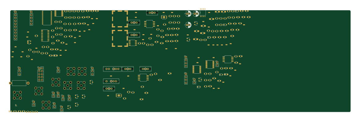
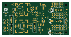
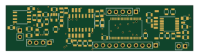
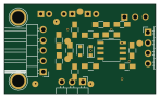
SWTEST is an open source PCB design by JasMoH, published on GitHub under the GPL-3.0 license. It is a 2-layer board measuring 17.4 × 17.7 mm, with 5 components from 4 distinct parts.
By type, the board carries 2 switches, 2 capacitors and 1 resistor.
From the project
Photoacoustic spectroscopy
SWTEST bill of materials (BOM)
5 components, 4 distinct parts — part numbers from the project's BOM.
| Qty | Part | Footprint | Refs |
|---|---|---|---|
| 1 | SP3T | SP3T_CK_SS-14D0839-VG | S1 |
| 1 | SP4T | SP4T_C&K_SS-14D0839-VG | S2 |
| 2 | C | C_0201 | C1, C2 |
| 1 | R | R_0201 | R1 |
SWTEST design files
The KiCad project lives in the JasMoH/Photoacoustic repository on GitHub; these links point at the commit this page was built from.
SWTEST: common questions
How big is the SWTEST PCB?
The SWTEST measures 17.4 × 17.7 mm, has 2 copper layers and is 1.6 mm thick.
How many components are on the SWTEST?
5 components, from 4 distinct parts, with part numbers taken from the project's own BOM. The full bill of materials is listed on this page.
Where can I download the SWTEST design files?
From the JasMoH/Photoacoustic repository on GitHub, which has the KiCad layout and the BOM; the links under Design files point to each one.
Can I use the SWTEST design in my own project?
Yes, under the terms of its GPL-3.0 license, which JasMoH chose for the repository.