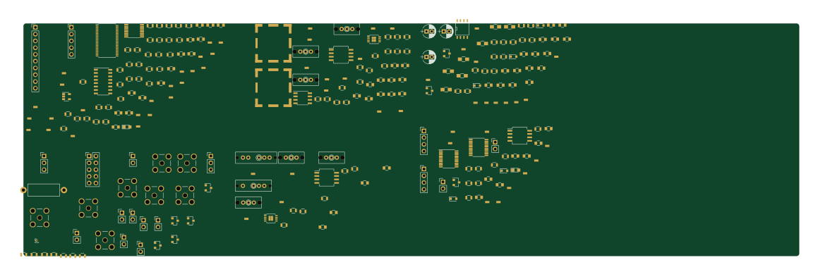
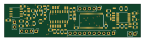
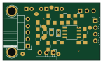
LNA test

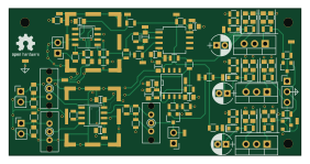
About the LNA test PCB
LNA test is an open source PCB design by JasMoH, published on GitHub under the GPL-3.0 license. It is a 2-layer board measuring 70.4 × 35.3 mm, with 109 components from 54 distinct parts.
Other key parts include the LM833, lm7805, LM7833, lm7905 and lmp7721. By type, the board carries 31 resistors, 28 capacitors, 18 connectors, 9 test points, 7 ICs and 7 inductors.
From the project
Photoacoustic spectroscopy
Main components on the LNA test
LNA test bill of materials (BOM)
109 components, 54 distinct parts — part numbers from the project's BOM.
| Qty | Part | Footprint | Refs |
|---|---|---|---|
| 1 | LM833 | SOIC-8-N | U1 |
| 1 | lm7805 | TO-220-3_Vertical | U2 |
| 1 | LM7833 | TO-220-3_Vertical | U3 |
| 1 | lm7905 | TO-220-3_Vertical | U4 |
| 1 | lmp7721 | SOIC-8_3.9x4.9mm_Pitch1.27mm | U6 |
| 1 | LM833 | SO-8_5.3x6.2mm_Pitch1.27mm | U7 |
| 1 | AD8429 | SOIC-8_3.9x4.9mm_Pitch1.27mm | U8 |
| 2 | DMN640L | SOT-23 | Q1, Q2 |
| 1 | vref-in | tyco_RCU_0603_Probe_Pad | J1 |
| 1 | vref | tyco_RCU_0603_Probe_Pad | J2 |
| 1 | V-IN | tyco_RCU_0603_Probe_Pad | J3 |
| 1 | GND | tyco_RCU_0603_Probe_Pad | J4 |
| 1 | V+IN | tyco_RCU_0603_Probe_Pad | J5 |
| 1 | +5V | tyco_RCU_0603_Probe_Pad | J6 |
| 1 | +3V3 | tyco_RCU_0603_Probe_Pad | J7 |
| 1 | -5V | tyco_RCU_0603_Probe_Pad | J8 |
| 1 | A IN | Pin_Header_Straight_1x02_Pitch2.54mm | J10 |
| 1 | B IN | Pin_Header_Straight_1x02_Pitch2.54mm | J11 |
| 1 | POWER_IN | Pin_Header_Straight_1x03_Pitch2.54mm | J12 |
| 1 | I IN | Pin_Header_Straight_1x02_Pitch2.54mm | J15 |
Show 34 more
| Qty | Part | Footprint | Refs |
|---|---|---|---|
| 2 | RF_Shield_One_Piece | SMS-201 | J17, J38 |
| 1 | +3V3 OUT | tyco_RCU_0603_Probe_Pad | J19 |
| 1 | AMP OUT | Pin_Header_Straight_1x02_Pitch2.54mm | J20 |
| 1 | -5V OUT | tyco_RCU_0603_Probe_Pad | J46 |
| 1 | +5V OUT | tyco_RCU_0603_Probe_Pad | J47 |
| 1 | A / I SEL | SPDT_OS102011MS2QN1 | S4 |
| 1 | B SEL | SPDT_OS102011MS2QN1 | S5 |
| 1 | LNA GAIN SEL | SPDT_OS102011MS2QN1 | S6 |
| 1 | CURRENT GUARD | tyco_RCU_0603_Probe_Pad | TP5 |
| 1 | CURRENT GUARD FB | tyco_RCU_0603_Probe_Pad | TP6 |
| 1 | LNA OUT | tyco_RCU_0603_Probe_Pad | TP7 |
| 1 | TIA GUARD BUFF IN | tyco_RCU_0603_Probe_Pad | TP8 |
| 1 | TIAV+ | tyco_RCU_0603_Probe_Pad | TP11 |
| 1 | GBUFFOUT | tyco_RCU_0603_Probe_Pad | TP12 |
| 1 | TIA_OUT | tyco_RCU_0603_Probe_Pad | TP13 |
| 1 | GBUFV- | tyco_RCU_0603_Probe_Pad | TP14 |
| 1 | GBUFFV+ | tyco_RCU_0603_Probe_Pad | TP15 |
| 3 | LED | D_0805 | D1, D2, D3 |
| 1 | BAT54S | SOT-23 | D9 |
| 7 | 10uH | L_0805 | L1, L2, L3, L4, L5, L6, L7 |
| 3 | 10u | CP_Radial_D5.0mm_P2.00mm | C1, C2, C5 |
| 7 | 0.1u | C_0805 | C3, C4, C20, C21, C35, C37, C38 |
| 14 | 0.1uF | C_0805 | C6, C7, C8, C9, C10, C11, C12, C13 +6 |
| 3 | 10pF | C_0805 | C25, C27, C36 |
| 1 | C | C_0805 | C39 |
| 4 | 10K | R_0805 | R1, R2, R46, R60 |
| 10 | 0 | R_0805 | R3, R4, R5, R6, R56, R57, R61, R62 +2 |
| 9 | 100 | R_0805 | R7, R8, R9, R43, R44, R45, R47, R58 +1 |
| 1 | 6.04 | R_0805 | R21 |
| 1 | 1M | R_0805 | R48 |
| 2 | 10M | R_0805 | R49, R50 |
| 1 | 100M | R_0805 | R55 |
| 2 | R | R_0805 | R59, R66 |
| 1 | CRT0805-BY-10R0ELF 0 Bourns | R_0805 | R108 |
LNA test design files
The KiCad project lives in the JasMoH/Photoacoustic repository on GitHub; these links point at the commit this page was built from.
LNA test: common questions
How big is the LNA test PCB?
The LNA test measures 70.4 × 35.3 mm, has 2 copper layers and is 1.6 mm thick.
How many components are on the LNA test?
109 components, from 54 distinct parts, with part numbers taken from the project's own BOM. The full bill of materials is listed on this page.
Where can I download the LNA test design files?
From the JasMoH/Photoacoustic repository on GitHub, which has the KiCad layout and the BOM; the links under Design files point to each one.
Can I use the LNA test design in my own project?
Yes, under the terms of its GPL-3.0 license, which JasMoH chose for the repository.