
Main v2

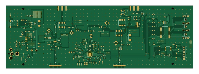
About the Main v2 PCB
Main v2 is an open source PCB design by JaxRaffnix, published on GitHub. It is a 4-layer board measuring 204.7 × 68.5 mm, with 189 components from 87 distinct parts.
Other key parts include the AP22811AW5-7, RMS-30+, SE2576L-R, HMC374 and PGA-103+. By type, the board carries 74 capacitors, 54 resistors, 17 connectors, 16 ICs, 11 inductors and 9 diodes.
It belongs with the rf & radio designs in this gallery.
Main components on the Main v2
Main v2 bill of materials (BOM)
189 components, 87 distinct parts — part numbers from the project's BOM.
| Qty | Part | Footprint | Refs |
|---|---|---|---|
| 1 | AP22811AW5-7 | SOT-23-5 | IC201 |
| 2 | RMS-30+ | RMS30 | IC301, IC402 |
| 1 | SE2576L-R | QFN50P300X300X90-17N-D | IC302 |
| 1 | HMC374 | SOT95P280X145-6N | IC401 |
| 1 | PGA-103+ | GVA63 | IC403 |
| 2 | PSA4-5043+ | PSA45043 | IC601, IC602 |
| 1 | 74LVC4T3144PWJ | SOP65P640X110-14N | IC701 |
| 1 | LTC6992CS6-4#TRMPBF | SOT95P280X100-6N | IC703 |
| 1 | 74LVC244AD-Q100J | SOIC127P1032X265-20N | IC704 |
| 1 | LT3042XMSE LT3042xMSE | MSOP-10-1EP_3x3mm_P0.5mm_EP1.68x1.88mm | U201 |
| 1 | TCCH-80+ | TCCH80 | U401 |
| 1 | ADF4351 | LFCSP-32-1EP_5x5mm_P0.5mm_EP3.25x3.25mm | U501 |
| 1 | PD0922J5050D2HF | PD0922J5050D2HF | U601 |
| 1 | XMB0220K1-50100G | XMB0220K1-50100G_TTT | U602 |
| 1 | DMP3068L-7 | SOT96P240X115-3N | Q201 |
| 1 | 2N7002 | SOT-23 | Q701 |
| 1 | ATX-11-F-26.000MHZ-F05-T | ATX11F26000MHZF05T | Y501 |
| 4 | Conn_Coaxial | SMA_Amphenol_132289_EdgeMount | J101, J102, J103, J104 |
| 1 | Barrel_Jack | BarrelJack_CUI_PJ-063AH_Horizontal_CircularHoles | J201 |
| 4 | CONMHF1-SMD-T | CONMHF1SMDT | J301, J401, J601, J602 |
Show 67 more
| Qty | Part | Footprint | Refs |
|---|---|---|---|
| 1 | CONN_01X06_PIN Conn_01x06_Pin | PinHeader_1x06_P2.54mm_Vertical | J701 |
| 4 | CONN_01X03_PIN Conn_01x03_Pin | PinHeader_1x03_P2.54mm_Vertical | J702, J704, J706, J708 |
| 3 | CONN_01X01_PIN Conn_01x01_Pin | PinHeader_1x01_P2.54mm_Vertical | J703, J705, J709 |
| 2 | 2450BP08A0100001T | 2450BP08A0100001T | FL301, FL401 |
| 1 | SYBP-92+ | SYBP92 | FL402 |
| 1 | LFCN-1800+ | LFCN1800 | FL601 |
| 1 | SW_DIP_X01 SW_DIP_x01 | SW_DIP_SPSTx01_Slide_6.7x4.1mm_W6.73mm_P2.54mm_LowProfile_JPin | SW201 |
| 1 | PESD5V0L1UL | D_SOD-882 | D201 |
| 7 | LED | LED_0805_2012Metric | D202, D203, D204, D205, D206, D301, D501 |
| 1 | SKY16602-632LF | SKY16602632LF | D401 |
| 1 | 28C0236-0JW-10 | LairdTech_28C0236-0JW-10 | FB201 |
| 2 | BLM18PG121SN1D | BLM18SP221SN1B | FB501, FB502 |
| 1 | LQG15HN1N5S02D | LQG15WH0N7B02D | L301 |
| 1 | 27 nH | L_0603_1608Metric | L401 |
| 1 | 12 nH | L_0402_1005Metric | L402 |
| 1 | 640 nH | L_0402_1005Metric | L403 |
| 2 | 7.5 nH | L_0402_1005Metric | L501, L502 |
| 2 | 47 nH | L_0402_1005Metric | L601, L602 |
| 1 | 1 uF | C_0603_1608Metric | C201 |
| 5 | 4.7 uF | C_0603_1608Metric | C202, C203, C206, C207, C208 |
| 1 | 0.1 uF | C_0603_1608Metric | C204 |
| 1 | 120 uF | CP_EIA-6032-20_AVX-F | C205 |
| 13 | 10 pF | C_0402_1005Metric | C301, C305, C406, C501, C504, C505, C508, C510 +5 |
| 9 | 100 pF | C_0402_1005Metric | C302, C303, C405, C408, C411, C602, C603, C605 +1 |
| 1 | 1 uF | C_0402_1005Metric | C304 |
| 4 | 1 nF | C_0402_1005Metric | C306, C513, C514, C527 |
| 1 | 2.2 pF | C_0402_1005Metric | C307 |
| 1 | 4.7 uF | C_0402_1005Metric | C308 |
| 2 | 15 pF | C_0402_1005Metric | C309, C409 |
| 1 | 100 nF | C_0402_1005Metric | C310 |
| 1 | 3.2 pF | C_0402_1005Metric | C311 |
| 2 | 2.4 pF | C_0402_1005Metric | C312, C313 |
| 1 | 4.7 uF | CP_EIA-6032-20_AVX-F | C401 |
| 1 | 1000 pF | C_0603_1608Metric | C402 |
| 3 | 150 pF | C_0402_1005Metric | C403, C404, C407 |
| 1 | 330 pF | C_0603_1608Metric | C410 |
| 1 | 330 pF | C_1206_3216Metric | C412 |
| 1 | 10 uF | C_1206_3216Metric | C413 |
| 13 | 0.1 uF | C_0402_1005Metric | C502, C503, C506, C507, C509, C520, C522, C523 +5 |
| 2 | 1 pF | C_0402_1005Metric | C511, C512 |
| 1 | 2.7 nF | C_0402_1005Metric | C516 |
| 1 | 39 nF | C_0402_1005Metric | C517 |
| 1 | 1.2 nF | C_0402_1005Metric | C518 |
| 3 | 120 pF | C_0402_1005Metric | C524, C525, C528 |
| 2 | 10 nF | C_0402_1005Metric | C601, C604 |
| 4 | 100K 100k | R_0603_1608Metric | R201, R202, R213, R303 |
| 5 | 1k | R_0603_1608Metric | R203, R204, R205, R212, R304 |
| 12 | 10K 10k | R_0603_1608Metric | R206, R503, R505, R506, R507, R515, R713, R714 +4 |
| 1 | 453 k | R_0603_1608Metric | R207 |
| 1 | 499 | R_0603_1608Metric | R208 |
| 1 | 49.9 k | R_0603_1608Metric | R209 |
| 1 | 150 | R_0603_1608Metric | R210 |
| 1 | 33.2K 33.2k | R_0603_1608Metric | R211 |
| 1 | 91 | R_0402_1005Metric | R301 |
| 4 | 0 | R_0603_1608Metric | R302, R501, R509, R510 |
| 1 | 26.7K | R_0603_1608Metric | R305 |
| 1 | 150R | R_0603_1608Metric | R401 |
| 2 | DNI | R_0603_1608Metric | R502, R504 |
| 1 | 100 | R_0603_1608Metric | R508 |
| 1 | 51 | R_0603_1608Metric | R511 |
| 1 | 680 | R_0603_1608Metric | R512 |
| 1 | 360 | R_0603_1608Metric | R513 |
| 1 | 4.7 k | R_0603_1608Metric | R514 |
| 1 | 100 | R_0402_1005Metric | R601 |
| 1 | 200 | R_0402_1005Metric | R602 |
| 11 | 100R | R_0603_1608Metric | R701, R702, R703, R704, R705, R706, R707, R708 +3 |
| 1 | 50K 50k | R_0603_1608Metric | R712 |
Main v2 design files
The KiCad project lives in the JaxRaffnix/sdr-analog-frontend repository on GitHub; these links point at the commit this page was built from.
Main v2: common questions
How big is the Main v2 PCB?
The Main v2 measures 204.7 × 68.5 mm, has 4 copper layers and is 1.579 mm thick.
How many components are on the Main v2?
189 components, from 87 distinct parts, with part numbers taken from the project's own BOM. The full bill of materials is listed on this page.
Where can I download the Main v2 design files?
From the JaxRaffnix/sdr-analog-frontend repository on GitHub, which has the KiCad layout, the schematic and the BOM; the links under Design files point to each one.
Can I use the Main v2 design in my own project?
The repository has no license, so all rights stay with JaxRaffnix. Use it as a reference, and ask the author before reusing the design.
Similar boards
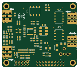
Hat
pa3gsb
65 × 56 mm81 parts2LNo license675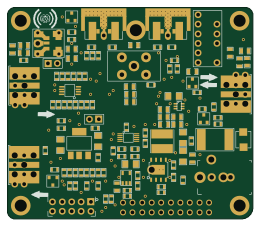
Radioberry preamp
65 × 56 mm137 parts2LNo license675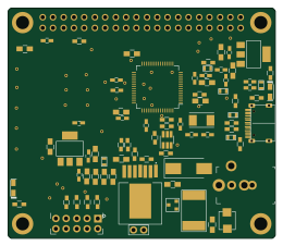
Radioberry juice
65 × 56 mm87 parts2LNo license675
Goodwatch20
travisgoodspeed
25.6 × 27.6 mm20 parts2LNo license568
GoodPocketWatch
75.2 × 101.2 mm56 parts2LNo license568
Goodwatch31
25.6 × 27.6 mm23 parts2LNo license568