
IoT putting analysis


About the IoT putting analysis PCB
IoT putting analysis is an open source Nordic nRF PCB design by JensenK17, published on GitHub. It is a 2-layer board measuring 22 × 22 mm, with 24 components from 11 distinct parts.
Its main chip is the NRF52820-QDXX, from the Nordic nRF family. Other key parts include the LSM6DS3 and LDO40LPU33RY. By type, the board carries 16 capacitors, 3 ICs, 3 resistors, 1 crystal and 1 battery holder.
It belongs with the iot & wireless, sensors and power & battery designs in this gallery.
From the project
Repo for full stack embedded edge AI putting stroke feedback system.
A comprehensive full-stack embedded edge AI putting stroke feedback system featuring real-time biomechanical analysis, custom PCB hardware, and multiple client applications.
This project implements a complete IoT ecosystem for putting stroke analysis:
- Arduino Firmware: Real-time IMU data processing and biomechanical feature extraction - Custom PCB: Ultra-compact hardware with nRF52820 BLE microcontroller and LSM6DS3 IMU - Mobile App: React Native/Expo application for data visualization and session management - Web App: Next.js web application with Web Bluetooth API support - Manufacturing…
Main components on the IoT putting analysis
IoT putting analysis bill of materials (BOM)
24 components, 11 distinct parts — part numbers from the project's BOM.
| Qty | Part | Footprint | Refs |
|---|---|---|---|
| 1 | NRF52820-QDXX nRF52820-QDxx | QFN-40-1EP_5x5mm_P0.4mm_EP3.6x3.6mm | U1 |
| 1 | LSM6DS3 | LGA-14_3x2.5mm_P0.5mm_LayoutBorder3x4y | U2 |
| 1 | LDO40LPU33RY | DFN-6-1EP_3x3mm_P0.95mm_EP1.7x2.6mm | U3 |
| 1 | 32MHZ 32MHz | Crystal_SMD_3225-4Pin_3.2x2.5mm | Y1 |
| 1 | 3.7V Ultra-Thin LiPo Battery | JST_PH_S2B-PH-SM4-TB_1x02-1MP_P2.00mm_Horizontal | BT1 |
| 2 | 18PF 18pF | C_01005_0402Metric | C1, C2 |
| 2 | 1µF | C_0603_1608Metric | C3, C5 |
| 1 | 10µF | C_0603_1608Metric | C4 |
| 11 | 0.1µF | C_01005_0402Metric | C6, C7, C8, C9, C10, C11, C12, C13 +3 |
| 1 | 10kΩ | R_0402_1005Metric | R1 |
| 2 | 4.7kΩ | R_0402_1005Metric | R2, R3 |
IoT putting analysis design files
The KiCad project lives in the JensenK17/ioT_putting_analysis repository on GitHub; these links point at the commit this page was built from.
IoT putting analysis: common questions
What microcontroller does the IoT putting analysis use?
The IoT putting analysis is built around the NRF52820-QDXX, from the Nordic nRF family.
How big is the IoT putting analysis PCB?
The IoT putting analysis measures 22 × 22 mm, has 2 copper layers and is 1.6 mm thick.
How many components are on the IoT putting analysis?
24 components, from 11 distinct parts, with part numbers taken from the project's own BOM. The full bill of materials is listed on this page.
Where can I download the IoT putting analysis design files?
From the JensenK17/ioT_putting_analysis repository on GitHub, which has the KiCad layout, the schematic and the BOM; the links under Design files point to each one.
Can I use the IoT putting analysis design in my own project?
The repository has no license, so all rights stay with JensenK17. Use it as a reference, and ask the author before reusing the design.
Can I test firmware for the IoT putting analysis without the hardware?
Yes. HardLabs builds a simulation of the board from its netlist and BOM, so you can run and debug Nordic nRF firmware against it before you order a PCB.
Similar boards
 Nordic nRF
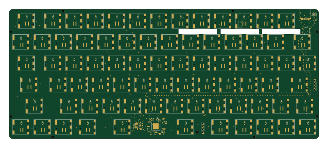
Keyboard
byrantech
262.5 × 109.6 mm206 parts2LMIT4.3k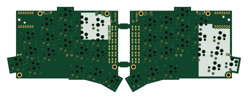 Nordic nRF
TOTEM
GEIGEIGEIST
258.8 × 94.4 mm85 parts2LCERN-OHL-P-2.02.0k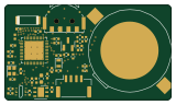 Nordic nRF
Pixl.js
solosky
40 × 23 mm45 parts4LGPL-2.01.4k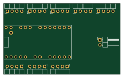 Nordic nRF
Board hl15-latest
dennisss
61 × 37 mm14 parts2LApache-2.0381 Nordic nRF
Board
363 × 128 mm420 parts4LApache-2.0381 Nordic nRF
Management
101 × 31.5 mm50 parts2LApache-2.0381