
HSprobe-REDFit adapter

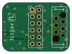
About the HSprobe-REDFit adapter PCB
HSprobe-REDFit adapter is an open source PCB design by JitterCompany, published on GitHub under the MIT license. It is a 2-layer board measuring 25 × 18 mm, with 3 components from 3 distinct parts.
From the project
Collection of useful utility PCBs for development purposes
KiCad projects for the small debug, programming and test boards used across Jitter projects. Each board has its own folder; manufacturing files are in production/.
Most Jitter boards expose a single 6-pin Würth REDFIT IDC SKEDD footprint that carries both SWD and a UART. SKEDD connectors press straight into plated holes, so the target board needs no mating connector. The adapters below convert a debug probe's native header to that 6-pin cable.
HSprobe-REDFit adapter bill of materials (BOM)
3 components, 3 distinct parts.
| Qty | Part | Footprint | Refs |
|---|---|---|---|
| 1 | FLE-107-01-G-DV Samtec | PinSocket_2x07_P1.27mm_Vertical_SMD | J1 |
| 1 | Conn_01x12_Male | PinHeader_2x06_P2.54mm_Vertical | J2 |
| 1 | DNI | WR-WST_REDFIT-6-pins_490107670612-adapter_to_pcb | J3 |
HSprobe-REDFit adapter design files
The KiCad project lives in the JitterCompany/debug-tools repository on GitHub; these links point at the commit this page was built from.
HSprobe-REDFit adapter: common questions
How big is the HSprobe-REDFit adapter PCB?
The HSprobe-REDFit adapter measures 25 × 18 mm, has 2 copper layers and is 1.6 mm thick.
How many components are on the HSprobe-REDFit adapter?
3 components, from 3 distinct parts. The full bill of materials is listed on this page.
Where can I download the HSprobe-REDFit adapter design files?
From the JitterCompany/debug-tools repository on GitHub, which has the KiCad layout and the schematic; the links under Design files point to each one.
Can I use the HSprobe-REDFit adapter design in my own project?
Yes, under the terms of its MIT license, which JitterCompany chose for the repository.
More boards in debug-tools
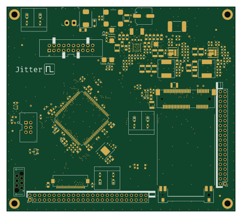 STM32
SL23 modem tester
120 × 107 mm195 parts4LMIT0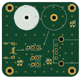
USBSwitch
41 × 40 mm13 parts2LMIT0
JLink-REDfit adapter
27.4 × 26 mm5 parts2LMIT0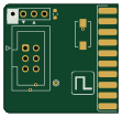
Jlink to TC2030-IDC microchip adapter
27.4 × 26 mm5 parts2LMIT0
BMP-REDFit adapter
22.9 × 16.5 mm4 parts2LMIT0
JTAG-SWD
16.5 × 12.7 mm3 parts2LMIT0