
ATtiny85 development board

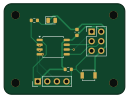
About the ATtiny85 development board
ATtiny85 development board is an open source AVR/Arduino PCB design by JunctionEDA, published on GitHub under the GPL-3.0 license. It is a 2-layer board measuring 32 × 24 mm, with 8 components from 8 distinct parts.
Its main chip is the ATtiny85-20S, from the AVR/Arduino family. By type, the board carries 2 connectors, 2 resistors, 1 IC, 1 switch, 1 diode and 1 capacitor.
It belongs with the dev boards & breakouts designs in this gallery.
From the project
Junction mechanical CAD: collaborative part studios, assemblies, and multi-file projects
Sync server for Junction — real-time multiplayer editing for KiCad.
One Rust binary (axum + tokio + sqlx) plus Postgres. Live at https://kicad-collab-production.up.railway.app.
Server-authoritative, Figma-style — not a CRDT:
- One in-memory document actor per open document, serializing all writes. - Each op gets the next per-doc sequence number and is durably inserted before it is acked or broadcast, so anything a client ever saw survives a crash. - Conflict resolution is property-level last-writer-wins, applied by clients in sequence order. The server never inspects or transforms change…
Main components on the ATtiny85 development board
ATtiny85 development board bill of materials (BOM)
8 components, 8 distinct parts.
| Qty | Part | Footprint | Refs |
|---|---|---|---|
| 1 | ATtiny85-20S | SOIC-8_5.3x5.3mm_P1.27mm | U1 |
| 1 | AVR-ISP-6 | PinHeader_2x03_P2.54mm_Vertical | J1 |
| 1 | IO | PinHeader_1x04_P2.54mm_Vertical | J2 |
| 1 | RESET | SW_SPST_B3U-1000P | SW1 |
| 1 | LED | LED_0805_2012Metric | D1 |
| 1 | 100n | C_0603_1608Metric | C1 |
| 1 | 10k | R_0603_1608Metric | R1 |
| 1 | 330 | R_0603_1608Metric | R2 |
ATtiny85 development board design files
The KiCad project lives in the JunctionEDA/junctioncad repository on GitHub; these links point at the commit this page was built from.
ATtiny85 development board: common questions
What microcontroller does the ATtiny85 development board use?
The ATtiny85 development board is built around the ATtiny85-20S, from the AVR/Arduino family.
How big is the ATtiny85 development board?
The ATtiny85 development board measures 32 × 24 mm, has 2 copper layers and is 1.6 mm thick.
How many components are on the ATtiny85 development board?
8 components, from 8 distinct parts. The full bill of materials is listed on this page.
Where can I download the ATtiny85 development board design files?
From the JunctionEDA/junctioncad repository on GitHub, which has the KiCad layout and the schematic; the links under Design files point to each one.
Can I use the ATtiny85 development board design in my own project?
Yes, under the terms of its GPL-3.0 license, which JunctionEDA chose for the repository.
Can I test firmware for the ATtiny85 development board without the hardware?
Yes. HardLabs builds a simulation of the board from its netlist and BOM, so you can run and debug AVR/Arduino firmware against it before you order a PCB.
More boards in junctioncad
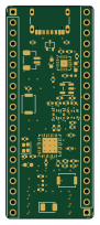 ESP32
Esp32
21 × 51 mm50 parts4LGPL-3.01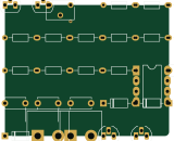
Ampli ht
40 × 32 mm29 parts2LGPL-3.01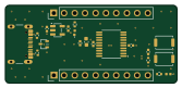 STM32
Stm32-usbc devboard
41.8 × 19 mm22 parts2LGPL-3.01
Blinker.guided
42 × 27 mm12 parts2LGPL-3.01
Blinker
42 × 27 mm12 parts2LGPL-3.01
USB-C 3.3 V regulator
34 × 22 mm9 parts2LGPL-3.01
Keyboard-2x2
35 × 15 mm8 parts2LGPL-3.01
I2C temperature sensor breakout
26 × 18 mm6 parts2LGPL-3.01
Six layer unrouted
20 × 20 mm4 parts6LGPL-3.01
Similar boards
 AVR/Arduino
Magspoof
samyk
35 × 29 mm11 parts2LNo license4.2k AVR/Arduino
Redox keyboard
mattdibi
162.2 × 126.5 mm77 parts2LMIT2.0k AVR/Arduino
Labrador
espotek-org
36.8 × 34.7 mm75 parts2LNo license1.2k AVR/Arduino
ModuleV450
stuartpittaway
30 × 61.4 mm39 parts2LCC-BY-NC-4.01.1k AVR/Arduino
V4
30 × 50 mm38 parts2LCC-BY-NC-4.01.1k AVR/Arduino
Discipline
coseyfannitutti
304.9 × 122.8 mm170 parts2LCC-BY-NC-4.01.0k