
Powerbank

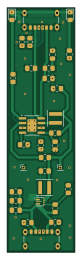
About the Powerbank PCB
Powerbank is an open source PCB design by k-off, published on GitHub under the Apache-2.0 license. It is a 2-layer board measuring 17.9 × 64.9 mm, with 30 components from 19 distinct parts.
Other key parts include the TPS61022 and IP2312-ESOP8. By type, the board carries 13 resistors, 9 capacitors, 2 ICs, 2 connectors, 2 diodes and 2 inductors.
It belongs with the power & battery designs in this gallery.
From the project
Minimal DIY Powerbank 1S4P USB-C 15W (3A)
Minimal DIY power bank with USB-C and fast charging.
This minimal DIY power bank features a custom-designed case created in Fusion 360 to securely hold four 18650 lithium-ion cells, providing a robust and compact power source. The enclosure is tailored to fit the battery pack and the custom PCB, ensuring a neat and durable assembly. The PCB, designed in KiCad, incorporates the IP2312 charging IC for safe and efficient battery charging and the Texas Instruments TPS61022 boost converter to step up the battery voltage to a stable 5 V output. Both the USB-C input and output ports support up to…
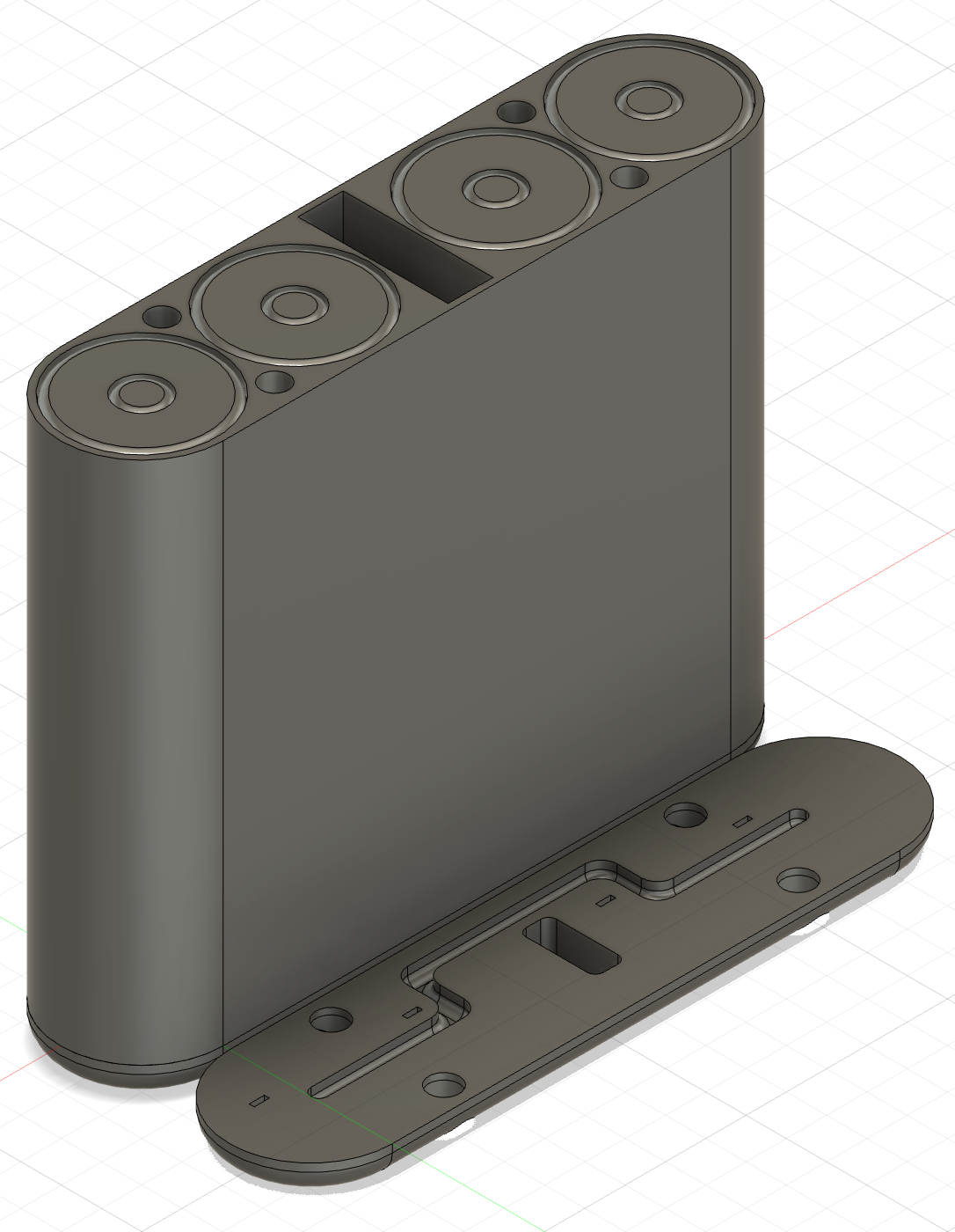
Main components on the Powerbank
Powerbank bill of materials (BOM)
30 components, 19 distinct parts.
| Qty | Part | Footprint | Refs |
|---|---|---|---|
| 1 | TPS61022 | Texas_RWU0007A_VQFN-7_2x2mm_P0.5mm | U1 |
| 1 | IP2312-ESOP8 | SOIC-8-1EP_3.9x4.9mm_P1.27mm_EP2.41x3.3mm_ThermalVias | U2 |
| 1 | USB_C_OUT | USB_C_Receptacle_GCT_USB4125-xx-x_6P_TopMnt_Horizontal | J1 |
| 1 | USB_C_IN | USB_C_Receptacle_GCT_USB4125-xx-x_6P_TopMnt_Horizontal | J2 |
| 1 | LED_RED | LED_0805_2012Metric_Pad1.15x1.40mm_HandSolder | D1 |
| 1 | LED_BLUE | LED_0805_2012Metric_Pad1.15x1.40mm_HandSolder | D2 |
| 2 | 1uH | L_Coilcraft_XxL4030 | L1, L2 |
| 3 | 10uF | C_0805_2012Metric_Pad1.18x1.45mm_HandSolder | C1, C4, C5 |
| 6 | 22uF | C_0805_2012Metric_Pad1.18x1.45mm_HandSolder | C2, C3, C6, C7, C8, C9 |
| 1 | 732k | R_0805_2012Metric_Pad1.20x1.40mm_HandSolder | R1 |
| 1 | 100k | R_0805_2012Metric_Pad1.20x1.40mm_HandSolder | R2 |
| 2 | 10k | R_0805_2012Metric_Pad1.20x1.40mm_HandSolder | R3, R4 |
| 2 | 5.1k | R_0805_2012Metric_Pad1.20x1.40mm_HandSolder | R6, R7 |
| 1 | 51k | R_0805_2012Metric_Pad1.20x1.40mm_HandSolder | R8 |
| 2 | 500R | R_0805_2012Metric_Pad1.20x1.40mm_HandSolder | R9, R10 |
| 1 | 1k | R_0805_2012Metric_Pad1.20x1.40mm_HandSolder | R11 |
| 1 | 45k | R_0805_2012Metric_Pad1.20x1.40mm_HandSolder | R12 |
| 1 | 0.5R | R_0805_2012Metric_Pad1.20x1.40mm_HandSolder | R13 |
| 1 | 2R | R_0805_2012Metric_Pad1.20x1.40mm_HandSolder | R14 |
Powerbank design files
The KiCad project lives in the k-off/powerbank repository on GitHub; these links point at the commit this page was built from.
Powerbank: common questions
How big is the Powerbank PCB?
The Powerbank measures 17.9 × 64.9 mm, has 2 copper layers and is 1.600198 mm thick.
How many components are on the Powerbank?
30 components, from 19 distinct parts. The full bill of materials is listed on this page.
Where can I download the Powerbank design files?
From the k-off/powerbank repository on GitHub, which has the KiCad layout and the schematic; the links under Design files point to each one.
Can I use the Powerbank design in my own project?
Yes, under the terms of its Apache-2.0 license, which k-off chose for the repository.
Similar boards
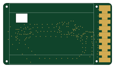
EinkPDA screen
TalismanDesign
95 × 54 mm27 parts2LApache-2.02.0k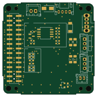
Stack chan
stack-chan
50 × 50 mm33 parts2LApache-2.01.7k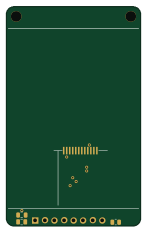
Display Carrier
AxxAxx
35.6 × 58.2 mm5 parts2LGPL-3.01.7k
ProgrammingAdapter
stuartpittaway
10.5 × 83 mm3 parts2LCC-BY-NC-4.01.1k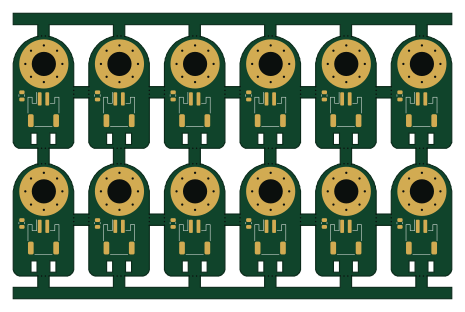
TemperaturePCB PANEL
116 × 75.5 mm178 parts2LCC-BY-NC-4.01.1k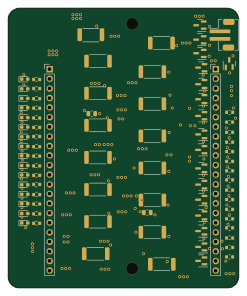
Module 16S PassiveBalanceAddOn
61 × 74 mm86 parts2LCC-BY-NC-4.01.1k