
Plan b

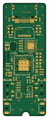
About the Plan b PCB
Plan b is an open source Nordic nRF PCB design by kaievns, published on GitHub. It is a 4-layer board measuring 16 × 42 mm, with 61 components from 38 distinct parts.
Its main chip is the nRF52840-QIAA, from the Nordic nRF family. Other key parts include the TPS22919DCKR. By type, the board carries 23 capacitors, 9 resistors, 7 connectors, 6 inductors, 4 ICs and 2 crystals.
It belongs with the keyboards and iot & wireless designs in this gallery.
From the project
Baking the ultimate split BLE keyboard PCB
This is a tiny opinionated PCB that has everything packed in one place for creating split bluetooth keyboards on top of nrf52840 chip and ZMK firmware
- an improved nice!nano clone in a smaller package - has baked nice!view inside with a slot for LCD - has baked in RGB controller - has baked in 6-pin SPI interface for external sensor - has baked in wiring for 6x6 keyboard matrix via JST connectors - has baked in power/reset switches for both sides - high efficiency DC/DC buck converters for all power lines - heavily fabrication optimised BOM and PCB (est $130 per 5 units at JLCPCB)
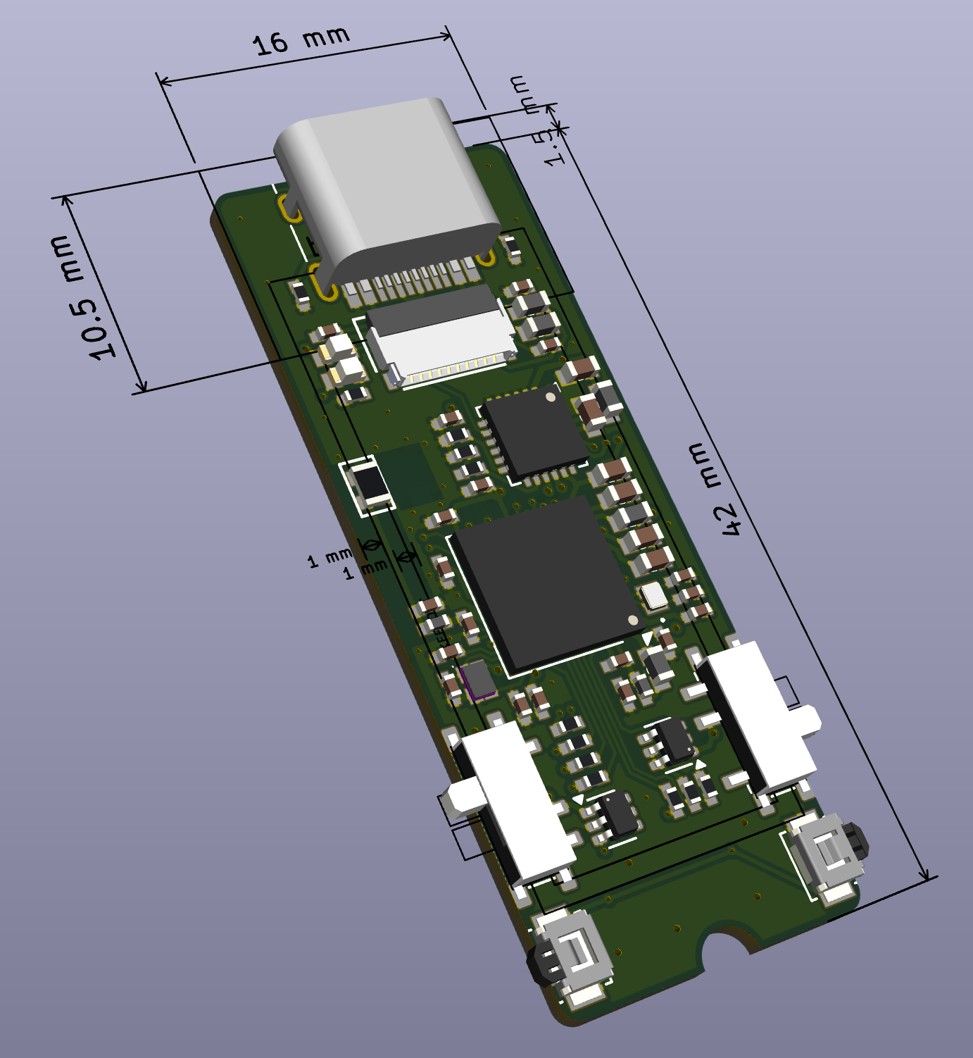
Main components on the Plan b
Plan b bill of materials (BOM)
61 components, 38 distinct parts.
| Qty | Part | Footprint | Refs |
|---|---|---|---|
| 1 | nRF52840-QIAA | Nordic_AQFN-73-1EP_7x7mm_P0.5mm | U1 |
| 1 | nRF52840-QIAA nPM1100-QDAx | QFN-24-1EP_4x4mm_P0.5mm_EP2.6x2.6mm_ThermalVias | U2 |
| 2 | TPS22919DCKR | SOT-363_SC-70-6 | U3, U4 |
| 1 | XTAL_SMD2016_32MHz_8pF_General 32MHz | OSCSC105P160X120X35-4N | X1 |
| 1 | XTAL_SMD3215_32.768kHz_9pF_General 32.768kHz | XTAL_ECS32761210TR | X2 |
| 1 | HRO_TYPE-C-31-M-12 | USB_C_Receptacle_HRO_TYPE-C-31-M-12 | J1 |
| 1 | Battery | JST_SH_SM02B-SRSS-TB_1x02-1MP_P1.00mm_Horizontal | J2 |
| 1 | rgb | JST_SH_SM03B-SRSS-TB_1x03-1MP_P1.00mm_Horizontal | J3 |
| 1 | columns | JST_SH_SM06B-SRSS-TB_1x06-1MP_P1.00mm_Horizontal | J4 |
| 1 | Conn_01x10 | CONN10x1_FH34SRJ-10S-0.5SH50_HIR | J5 |
| 1 | rows | JST_SH_SM06B-SRSS-TB_1x06-1MP_P1.00mm_Horizontal | J6 |
| 1 | sensor | JST_SH_SM06B-SRSS-TB_1x06-1MP_P1.00mm_Horizontal | J7 |
| 1 | ANT2012LL13R2400A | ANT2012LL13R2400A | AE1 |
| 4 | 100k | R_0402_1005 | R_BLE1, R_BLE2, R_DIV1, R_DIV2 |
| 1 | 5k1 | R_0402_1005 | R_ICHG1 |
| 1 | Power | Switch_MSK12C02 | SW1 |
| 1 | Reset | SW_SPST_B3U-3000P-B | SW2 |
| 1 | L0603G (Amber) | LED_0603_1608 | LD2 |
| 1 | L0603 (Blue) | LED_0603_1608 | LD3 |
| 2 | 600R | F_0603_1608 | FB1, FB2 |
Show 18 more
| Qty | Part | Footprint | Refs |
|---|---|---|---|
| 1 | L0402-4n7 4.7 nH | L_0402_1005 | L1 |
| 2 | L0603-10µ 10µH | L_0603_1608 | L2, L4 |
| 1 | L0402-15n 15nH | L_0402_1005 | L3 |
| 4 | C0402-12p 12pF | C_0402_1005 | C1, C2, C17, C18 |
| 1 | C0402-0.8p 0.8 pF | C_0402_1005 | C3 |
| 1 | C0402-0.8p 0.5 pF | C_0402_1005 | C4 |
| 4 | C0402-100n 100nF | C_0402_1005 | C5, C7, C8, C12 |
| 2 | C0603-4µ7-6.3V-X7R 4.7µF | C_0603_1608 | C6, C20 |
| 1 | C0402-100n 820pF | C_0402_1005 | C9 |
| 1 | C0402-100p 100pF | C_0402_1005 | C11 |
| 2 | C0603-1µ0 1.0µF | C_0402_1005 | C14, C15 |
| 1 | C0402-47n 47nF | C_0402_1005 | C16 |
| 1 | C0603-4µ7-10V-X7S 10µF | C_0603_1608 | C19 |
| 1 | C0603-4µ7-10V-X7S 4.7µF | C_0603_1608 | C21 |
| 3 | 1.0µF | C_0402_1005 | C22, C30, C38 |
| 1 | 560pF | C_0402_1005 | C37 |
| 4 | 5k1 | R_0402_1005 | R3, R21, R22, R33 |
| 5 | 100R | R_0402_1005 | R8, R11, R14, R15, R16 |
Plan b design files
The KiCad project lives in the kaievns/plan-b repository on GitHub; these links point at the commit this page was built from.
- Layoutplan-b.kicad_pcb
- Schematicplan-b.kicad_sch
Plan b: common questions
What microcontroller does the Plan b use?
The Plan b is built around the nRF52840-QIAA, from the Nordic nRF family.
How big is the Plan b PCB?
The Plan b measures 16 × 42 mm, has 4 copper layers and is 1.1412 mm thick.
How many components are on the Plan b?
61 components, from 38 distinct parts. The full bill of materials is listed on this page.
Where can I download the Plan b design files?
From the kaievns/plan-b repository on GitHub, which has the KiCad layout and the schematic; the links under Design files point to each one.
Can I use the Plan b design in my own project?
The repository has no license, so all rights stay with kaievns. Use it as a reference, and ask the author before reusing the design.
Can I test firmware for the Plan b without the hardware?
Yes. HardLabs builds a simulation of the board from its netlist and BOM, so you can run and debug Nordic nRF firmware against it before you order a PCB.
Similar boards
 Nordic nRF
Keyboard
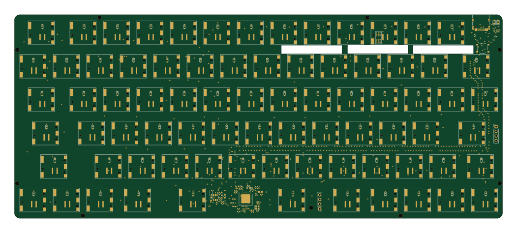
byrantech
262.5 × 109.6 mm206 parts2LMIT4.3k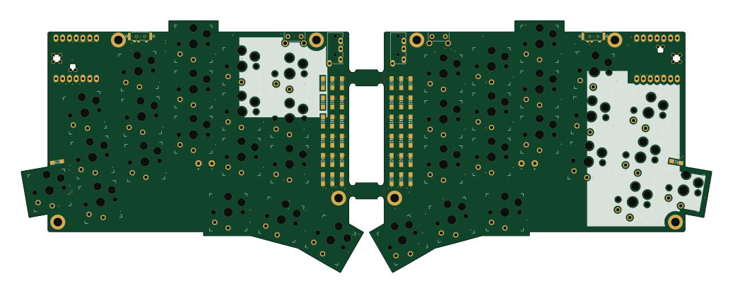 Nordic nRF
TOTEM
GEIGEIGEIST
258.8 × 94.4 mm85 parts2LCERN-OHL-P-2.02.0k Nordic nRF
Pixl.js
solosky
40 × 23 mm45 parts4LGPL-2.01.4k Nordic nRF
Management
dennisss
101 × 31.5 mm50 parts2LApache-2.0381 Nordic nRF
Board
363 × 128 mm420 parts4LApache-2.0381 Nordic nRF
Board hl15-latest
61 × 37 mm14 parts2LApache-2.0381