
Main PCB 2.0

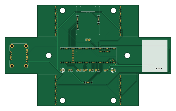
About the Main PCB 2.0
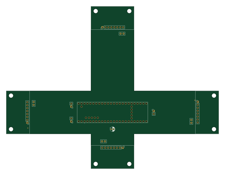
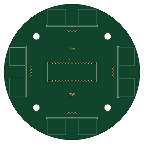
Main PCB 2.0 is an open source NXP PCB design by Kushal-Sachdeva78, published on GitHub under the MIT license. It is a 2-layer board measuring 180 × 110 mm, with 15 components from 9 distinct parts.
Its main chip is the TEENSY 4.1, from the NXP family. By type, the board carries 6 connectors, 2 capacitors and 1 IC.
It belongs with the robotics & motion and sensors designs in this gallery.
From the project
Autonomous RoboCupJunior Soccer (IR League) robots by Team VVS Ballers: 9th place at RoboCup 2026 in Incheon. Teensy 4.1 multi-board electronics, IR/line/ultrasonic sensing, OpenMV vision, 48 V solenoid kicker. Firmware, KiCad PCBs, Fusion 360 CAD.
KiCad sources, Gerbers, drill and job files for every board, plus human-readable wiring and ready-to-order fab packages.
The previous main board revision is archived in ../Legacy/PCB/Mainv1`.
Each board folder is a KiCad project — open the .kicadpro (the matching .kicadpcb and .kicadsch sit beside it). The loose .gbr / .drl / .gbrjob files are generated fabrication outputs; for ordering, prefer the zipped packages in Fabrication/. KiCad local-settings files (.kicadprl) and auto-backups are intentionally git-ignored.
Main components on the Main PCB 2.0
Main PCB 2.0 bill of materials (BOM)
15 components, 9 distinct parts — part numbers from the project's BOM.
| Qty | Part | Footprint | Refs |
|---|---|---|---|
| 1 | TEENSY 4.1 TEENSY_4.1 | TEENSY41 | IC1 |
| 4 | Conn_01x13 | PinHeader_1x13_P2.54mm_Vertical | J1, J2, J3, J4 |
| 1 | Conn_01x06 | PinHeader_1x06_P2.54mm_Vertical | J5 |
| 1 | Conn_01x04 | PinHeader_1x04_P2.54mm_Vertical | J6 |
| 3 | Conn_01x02 | PinHeader_1x02_P2.54mm_Vertical | 3.3V_Power1, 5V_Power1, Camera1 |
| 1 | BNO055 | MODULE_2472 | Gyro_Sensor1 |
| 1 | Conn_01x03 | PinHeader_1x03_P2.54mm_Vertical | Solenoid1 |
| 1 | Conn_01x04 | PinHeader_1x04_P2.54mm_Vertical | Ultrasonic_Sensor1 |
| 2 | 104 | CP_Radial_D5.0mm_P2.50mm | C2, C3 |
Main PCB 2.0 design files
The KiCad project lives in the Kushal-Sachdeva78/VVS-Ballers-RoboCup repository on GitHub; these links point at the commit this page was built from.
Main PCB 2.0: common questions
What microcontroller does the Main PCB 2.0 use?
The Main PCB 2.0 is built around the TEENSY 4.1, from the NXP family.
How big is the Main PCB 2.0?
The Main PCB 2.0 measures 180 × 110 mm, has 2 copper layers and is 1.6 mm thick.
How many components are on the Main PCB 2.0?
15 components, from 9 distinct parts, with part numbers taken from the project's own BOM. The full bill of materials is listed on this page.
Where can I download the Main PCB 2.0 design files?
From the Kushal-Sachdeva78/VVS-Ballers-RoboCup repository on GitHub, which has the KiCad layout, the schematic and the BOM; the links under Design files point to each one.
Can I use the Main PCB 2.0 design in my own project?
Yes, under the terms of its MIT license, which Kushal-Sachdeva78 chose for the repository.
Can I test firmware for the Main PCB 2.0 without the hardware?
Yes. HardLabs builds a simulation of the board from its netlist and BOM, so you can run and debug NXP firmware against it before you order a PCB.
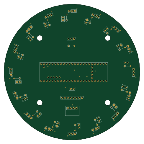
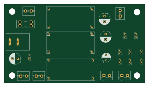
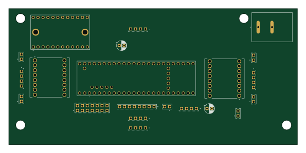
More boards in VVS-Ballers-RoboCup
Similar boards
 NXP
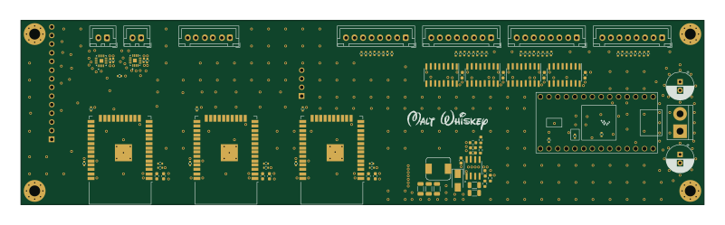
NXPMega-Cube-Board
MaltWhiskey
200 × 54 mm100 parts4LNo license763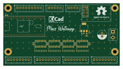 NXP
NXP32Bit shift register
100 × 54 mm56 parts4LNo license763 NXP
NXPICED-L
kiibohd
175.4 × 145 mm163 partsCERN-OHL-1.2415 NXP
NXPK-Type
357.5 × 131.8 mm361 partsCERN-OHL-1.2415 NXP
NXPIC60
285 × 95 mm242 partsCERN-OHL-1.2415 NXP
NXPWhiteFox
304.8 × 101.1 mm296 partsCERN-OHL-1.2415