
Power splitter

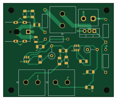
About the Power splitter PCB
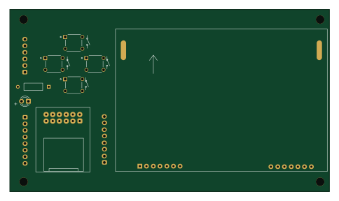
Power splitter is an open source PCB design by kylenmorris, published on GitHub. It is a 2-layer board measuring 57.1 × 48.5 mm, with 26 components from 10 distinct parts.
Other key parts include the AP62300TWU. By type, the board carries 10 capacitors, 5 connectors, 2 ICs, 2 fuses, 2 inductors and 2 resistors.
It belongs with the sensors and displays & leds designs in this gallery.
From the project
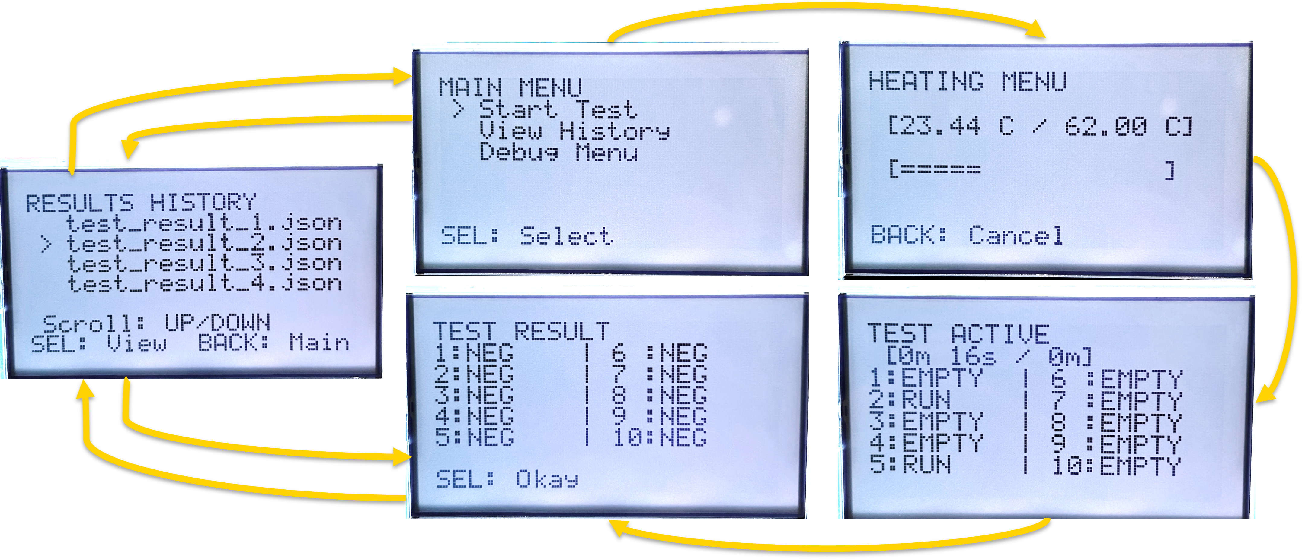
A custom reaction chamber for automation of crop pathogens testing using a NAAT reaction, developed as a capstone project
Our capstone project was to design a self-contained device that would run Nucleic Acid Amplification Testing (NAAT), a method of in-field crop disease testing that replaces slow lab-based testing. This project was introduced to us by PathoScan who supplied the reaction tubes and supplies.
This device has several features, including maintaining and monitoring of internal chamber temperature, light-emission monitoring, storage of test results, and input/output from the user.
Main components on the Power splitter
Power splitter bill of materials (BOM)
26 components, 10 distinct parts.
| Qty | Part | Footprint | Refs |
|---|---|---|---|
| 2 | AP62300TWU | TSOT-23-6 | U1, U2 |
| 1 | IRLZ44N | TO-220-3_Vertical | Q2 |
| 3 | B02P-VL | CONN_B02P-VL_JST | J1, J2, J3 |
| 1 | PJ-082BH | SAMESKY_PJ-082BH | J4 |
| 1 | B02P-VL | JST_NV_B02P-NV_1x02_P5.00mm_Vertical | J5 |
| 2 | TR/3216FF6.5-R | FUS_CB_3216FF | F1, F3 |
| 2 | R_Small | YAG_MF25_YAG | Thermal_Fuse_1, Thermal_Fuse_2 |
| 2 | L | L_Axial_L7.0mm_D3.3mm_P5.08mm_Vertical_Fastron_MICC | L1, L2 |
| 10 | C_Small | C_1206_3216Metric_Pad1.33x1.80mm_HandSolder | C1, C2, C3, C5, C6, C7, C8, C9 +2 |
| 2 | R_Small_US | YAG_MF25_YAG | R7, R8 |
Power splitter design files
The KiCad project lives in the kylenmorris/reaction-chamber repository on GitHub; these links point at the commit this page was built from.
Power splitter: common questions
How big is the Power splitter PCB?
The Power splitter measures 57.1 × 48.5 mm, has 2 copper layers and is 1.6 mm thick.
How many components are on the Power splitter?
26 components, from 10 distinct parts. The full bill of materials is listed on this page.
Where can I download the Power splitter design files?
From the kylenmorris/reaction-chamber repository on GitHub, which has the KiCad layout and the schematic; the links under Design files point to each one.
Can I use the Power splitter design in my own project?
The repository has no license, so all rights stay with kylenmorris. Use it as a reference, and ask the author before reusing the design.
More boards in reaction-chamber
Similar boards

LevelShifterBreakout
scottbez1
15.2 × 20.3 mm5 parts2LApache-2.022.2k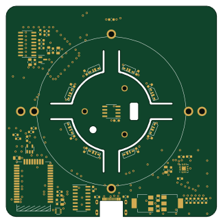
View base
81.2 × 81.2 mm81 parts2LApache-2.022.2k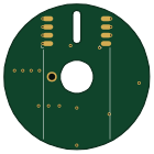
View screen
35 × 35 mm12 parts2LApache-2.022.2k
BM28B0.6-24DSBreakout
15.2 × 35.6 mm3 parts2LApache-2.022.2k
ChainlinkDriverTester
198.1 × 95.3 mm123 parts2LApache-2.04.2k
ChainlinkBase
98.4 × 190.5 mm119 parts2LApache-2.04.2k