
Layout

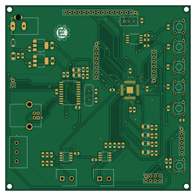
About the Layout PCB
Layout is an open source PIC PCB design by laurapellizari, published on GitHub. It is a 2-layer board measuring 100 × 100 mm, with 89 components from 41 distinct parts.
Its main chip is the PIC32MM0064GPM048-I_PT, from the PIC family. Other key parts include the LD1117DT50TR_SOT223, LD1117S33CTR_SOT223, MCP2200-I-SO and 24LC512-I_SM. By type, the board carries 34 resistors, 22 capacitors, 10 connectors, 5 ICs, 5 switches and 4 LEDs.
From the project
Embedded hardware design for learning
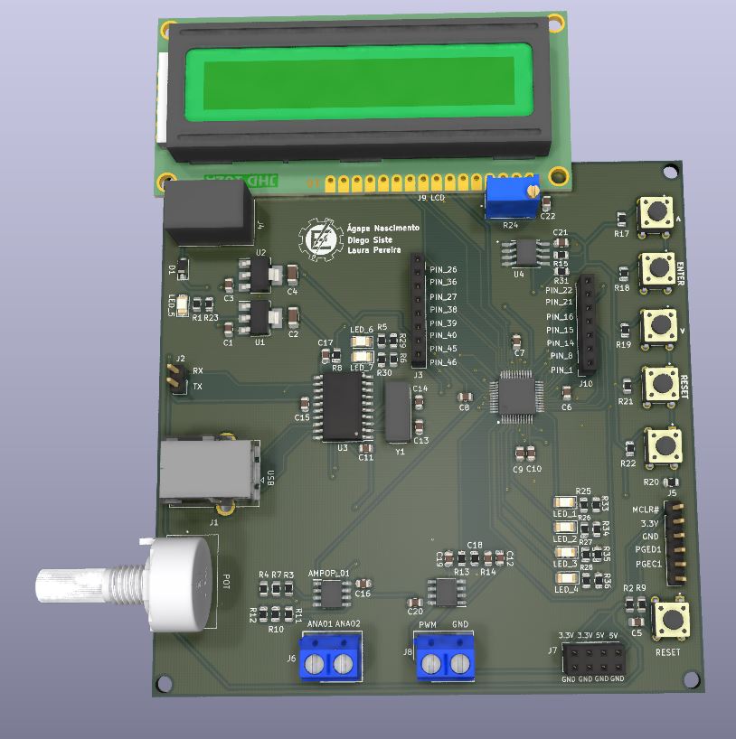
Main components on the Layout
Layout bill of materials (BOM)
89 components, 41 distinct parts.
| Qty | Part | Footprint | Refs |
|---|---|---|---|
| 1 | PIC32MM0064GPM048-I_PT | QFP50P900X900X120-49N | IC1 |
| 1 | LD1117DT50TR_SOT223 | SOT-223-3_TabPin2 | U1 |
| 1 | LD1117S33CTR_SOT223 | SOT-223-3_TabPin2 | U2 |
| 1 | MCP2200-I-SO | SOIC-20W_7.5x12.8mm_P1.27mm | U3 |
| 1 | 24LC512-I_SM | SOIC127P794X202-8N | U4 |
| 1 | 12MHz | XTAL_ECS-120-20-4X | Y1 |
| 1 | USB_B | USB_B_OST_USB-B1HSxx_Horizontal | J1 |
| 1 | Conn_01x02 | PinHeader_1x02_P2.54mm_Vertical | J2 |
| 1 | EXTENSÃO_2 | PinSocket_1x08_P2.54mm_Vertical | J3 |
| 1 | PJ-002A | CUI_PJ-002A | J4 |
| 1 | ICSP | PinHeader_1x06_P2.54mm_Vertical | J5 |
| 2 | OSTTA024163 | SHDR2W100P0X508_1X2_1086X900X1300P | J6, J8 |
| 1 | Conn_02x04_Top_Bottom | PinSocket_2x04_P2.54mm_Vertical | J7 |
| 1 | LDC_header | PinSocket_1x16_P2.54mm_Vertical | J9 |
| 1 | EXTENSÃO_1 | PinSocket_1x07_P2.54mm_Vertical | J10 |
| 1 | POT | P160KN0QD15B10K | -1 |
| 1 | SWL1 | SW_1825910-6-4 | MCLR1 |
| 2 | LM358DG | SOIC127P600X175-8N | OP1, OP2 |
| 5 | 1825910-6 | SW_1825910-6-4 | SW1, SW2, SW3, SW4, SW5 |
| 1 | LED_1 | LED_1206_3216Metric | LED_1 |
Show 21 more
| Qty | Part | Footprint | Refs |
|---|---|---|---|
| 1 | LED_ALIM | LED_1206_3216Metric | LED_5 |
| 1 | Lx_LED | LED_1206_3216Metric | LED_6 |
| 1 | Rx_LED | LED_1206_3216Metric | LED_7 |
| 1 | 1N5819 | D_SOD-123 | D1 |
| 1 | LED_2 | LED_1206_3216Metric | D2 |
| 1 | LED_3 | LED_1206_3216Metric | D3 |
| 1 | LED_4 | LED_1206_3216Metric | D4 |
| 14 | 100nF | C_0805_2012Metric | C1, C3, C5, C6, C7, C8, C10, C11 +6 |
| 2 | 10uF | C_1206_3216Metric | C2, C4 |
| 1 | 10uF | C_0805_2012Metric | C9 |
| 3 | 220nF | C_0805_2012Metric | C12, C18, C19 |
| 2 | 22pF | C_0805_2012Metric | C13, C14 |
| 7 | 56 | R_0805_2012Metric | R1, R29, R30, R33, R34, R35, R36 |
| 2 | 1k | R_0805_2012Metric | R2, R22 |
| 7 | 3k3 | R_0805_2012Metric | R3, R4, R7, R10, R11, R12, R21 |
| 9 | 100 | R_0805_2012Metric | R5, R6, R13, R14, R23, R25, R26, R27 +1 |
| 4 | 4k7 | R_0805_2012Metric | R8, R15, R19, R31 |
| 2 | 10k | R_0805_2012Metric | R9, R20 |
| 1 | 9k1 | R_0805_2012Metric | R17 |
| 1 | 6k8 | R_0805_2012Metric | R18 |
| 1 | POT_LCD | TRIM_3296W-1-103RLF | R24 |
Layout design files
The KiCad project lives in the laurapellizari/PBLE01---Hardware repository on GitHub; these links point at the commit this page was built from.
- LayoutVH3/VH3/VH3.kicad_pcb
Layout: common questions
What microcontroller does the Layout use?
The Layout is built around the PIC32MM0064GPM048-I_PT, from the PIC family.
How big is the Layout PCB?
The Layout measures 100 × 100 mm, has 2 copper layers and is 1.6 mm thick.
How many components are on the Layout?
89 components, from 41 distinct parts. The full bill of materials is listed on this page.
Where can I download the Layout design files?
From the laurapellizari/PBLE01---Hardware repository on GitHub, which has the KiCad layout; the links under Design files point to each one.
Can I use the Layout design in my own project?
The repository has no license, so all rights stay with laurapellizari. Use it as a reference, and ask the author before reusing the design.
Can I test firmware for the Layout without the hardware?
Yes. HardLabs builds a simulation of the board from its netlist and BOM, so you can run and debug PIC firmware against it before you order a PCB.
More boards in PBLE01---Hardware
 PIC
PICSub circ completo (2)
100 × 67 mm77 parts2LNo license0 PIC
PICSub circuito do microcontrolador
100 × 100 mm41 parts2LNo license0
Sub circ interface
2.8 × 2.8 mm19 parts2LNo license0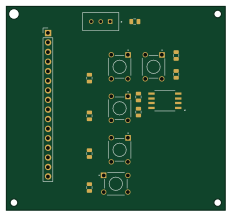
Sub circuito perifericos
58 × 54 mm17 parts2LNo license0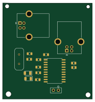
Sub circ de comunicacao
46.3 × 49.8 mm16 parts2LNo license0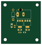
Sub Circuito de Alimentação
40.6 × 43.4 mm10 parts2LNo license0
Similar boards
 PIC
PICPslab hardware
fossasia
99 × 53.3 mm187 parts4LApache-2.01.7k PIC
PICLens
ervanalb
80 × 80 mm53 parts4LNo license515 PIC
PICMicro 8088
skiselev
152.4 × 101.6 mm71 partsGPL-3.0414 PIC
PICGB-LIVE32
Gekkio
51.4 × 61 mm46 parts4LCC-BY-4.0376 PIC
PICGB-MBCTEST
51.4 × 61 mm32 parts2LCC-BY-4.0376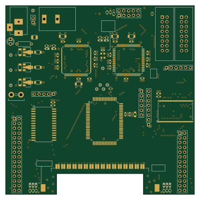 PIC
PICGB-BENCH-G1
100 × 100 mm98 parts4LCC-BY-4.0376