
Seedsigner luckfox devboard

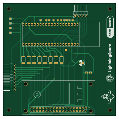
About the Seedsigner luckfox devboard PCB
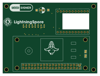
Seedsigner luckfox devboard is an open source Raspberry Pi PCB design by lightningspore, published on GitHub. It is a 2-layer board measuring 100 × 100 mm, with 19 components from 9 distinct parts.
Its main chip is the WAVESHARE_LCD_BUTTON_BOARD_1.3IN, from the Raspberry Pi family. Other key parts include the LuckFox_Pico. By type, the board carries 8 resistors, 2 ICs, 2 connectors, 2 jumpers and 1 capacitor.
It belongs with the dev boards & breakouts designs in this gallery.
From the project
Use an air-gapped Raspberry Pi Zero to sign for Bitcoin transactions! (and do other cool stuff)
SeedSigner code fork: https://github.com/lightningspore/seedsigner/tree/0.8.5-luckfox
Previous Iteration: LuckFox Pico Pro Max (More Flash, SPI Flash)
These example builds can build a device for around $60.
Replace /dev/diskX with your actual SD card device path.
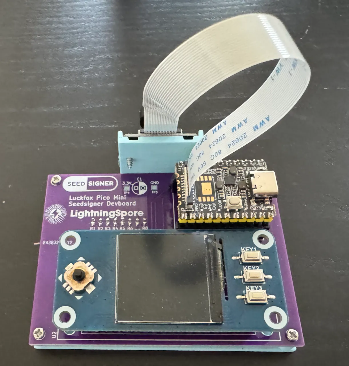
Main components on the Seedsigner luckfox devboard
Seedsigner luckfox devboard bill of materials (BOM)
19 components, 9 distinct parts — part numbers from the project's BOM.
| Qty | Part | Footprint | Refs |
|---|---|---|---|
| 1 | LuckFox_Pico | LUCKFOX_PICO_PRO_MAX_PTH | U1 |
| 1 | WAVESHARE_LCD_BUTTON_BOARD_1.3IN RASPBERRY_PI_3_MODEL_B+ | WAVESHARE_LCD_BUTTON | U2 |
| 1 | CONN_01X04 Conn_01x10 | PinHeader_1x10_P2.54mm_Horizontal | J1 |
| 1 | Conn_01x05 | PinHeader_1x05_P2.54mm_Horizontal | J2 |
| 4 | MountingHole | MOUNT_HOLE_3MM | H1, H2, H3, H4 |
| 1 | Jumper_2_Small_Bridged | SolderJumper-2_P1.3mm_Bridged_Pad1.0x1.5mm | JP1 |
| 1 | Jumper_2_Small_Open | SolderJumper-2_P1.3mm_Open_Pad1.0x1.5mm | JP2 |
| 1 | 0.1UF C_Polarized | CP_Radial_D5.0mm_P2.50mm | C1 |
| 8 | 10K R | R_2512_6332Metric | R1, R2, R3, R4, R5, R6, R7, R8 |
Seedsigner luckfox devboard design files
The KiCad project lives in the lightningspore/seedsigner-luckfox-pico repository on GitHub; these links point at the commit this page was built from.
Seedsigner luckfox devboard: common questions
What microcontroller does the Seedsigner luckfox devboard use?
The Seedsigner luckfox devboard is built around the WAVESHARE_LCD_BUTTON_BOARD_1.3IN, from the Raspberry Pi family.
How big is the Seedsigner luckfox devboard PCB?
The Seedsigner luckfox devboard measures 100 × 100 mm, has 2 copper layers and is 1.6 mm thick.
How many components are on the Seedsigner luckfox devboard?
19 components, from 9 distinct parts, with part numbers taken from the project's own BOM. The full bill of materials is listed on this page.
Where can I download the Seedsigner luckfox devboard design files?
From the lightningspore/seedsigner-luckfox-pico repository on GitHub, which has the KiCad layout, the schematic and the BOM; the links under Design files point to each one.
Can I use the Seedsigner luckfox devboard design in my own project?
The repository has no license, so all rights stay with lightningspore. Use it as a reference, and ask the author before reusing the design.
Can I test firmware for the Seedsigner luckfox devboard without the hardware?
Yes. HardLabs builds a simulation of the board from its netlist and BOM, so you can run and debug Raspberry Pi firmware against it before you order a PCB.
More boards in seedsigner-luckfox-pico
Similar boards
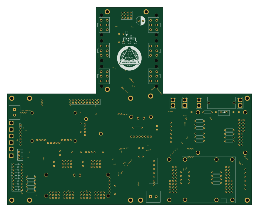 Raspberry Pi
Open source rover
nasa-jpl
220 × 178 mm144 parts2LApache-2.09.7k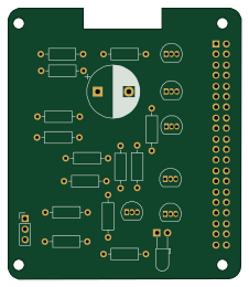 Raspberry Pi
Iot
dotnet
56 × 65 mm24 parts2LMIT2.4k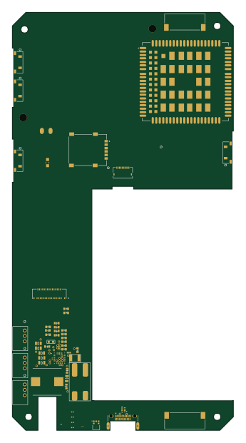 Raspberry Pi
SPIRIT
SPIRIT-org
82 × 155 mm130 parts6LCERN-OHL-S-2.01.3k Raspberry Pi
CM5RevEng
schlae
55 × 40 mm417 parts10LNo license1.0k Raspberry Pi
Haxo hw
cardonabits
102.4 × 211.3 mm38 parts2LCustom license673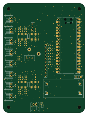 Raspberry Pi
Phased
Neumi
75 × 100 mm71 parts2LNo license507